Device and method for testing the quality of a display substrate

a technology for display substrates and test methods, which is applied in the direction of measurement devices, analysing solids using sonic/ultrasonic/infrasonic waves, instruments, etc. it can solve the problems of low reliability of testing, inability to determine whether the processing area has been broken in this testing method, and the production line and the products are damaged by the broken substrates, so as to facilitate the maintenance and repair of the production line

Inactive Publication Date: 2014-11-27
SHENZHEN CHINA STAR OPTOELECTRONICS TECH CO LTD
View PDF7 Cites 1 Cited by
  • Summary
  • Abstract
  • Description
  • Claims
  • Application Information

AI Technical Summary

Benefits of technology

The patent describes a device that can detect if there are any fragments on a substrate, and accurately locate them. This can help prevent damage to the substrate and products, and also provide clues to find the causes of the fragments and facilitate maintenance and repair of the production line. The device has an ultrasonic emitter and receiver that can rotate or move translationally to scan the substrate. The resulting data can be analyzed and displayed in real-time on a computer screen.

Problems solved by technology

Since the processing area on the substrate can't receive the reflected light well, it can't be determined whether the processing area has been broken.
Since the above comparison can't be implemented in the processing area, it also can't be determined whether the processing area has been broken in this testing method.
Thus the reliability of the testing is low and the broken substrates can't be found out entirely.

Method used


Image

  • Device and method for testing the quality of a display substrate
  • Device and method for testing the quality of a display substrate
  • Device and method for testing the quality of a display substrate

Examples


Embodiment Construction

[0033]The present invention may be further described in the following in detail with reference to the accompanying drawings and embodiments.

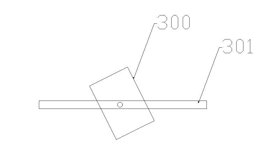
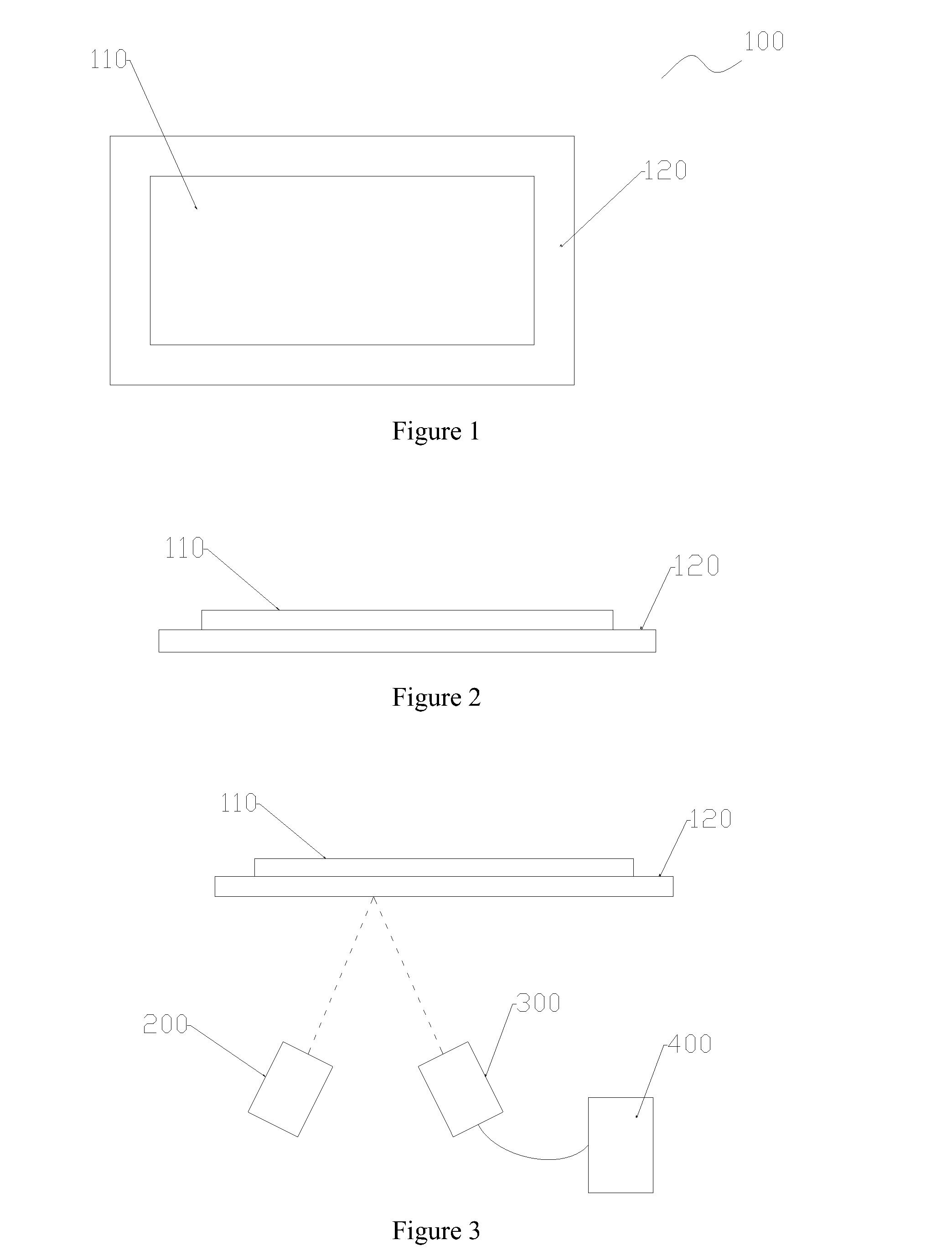
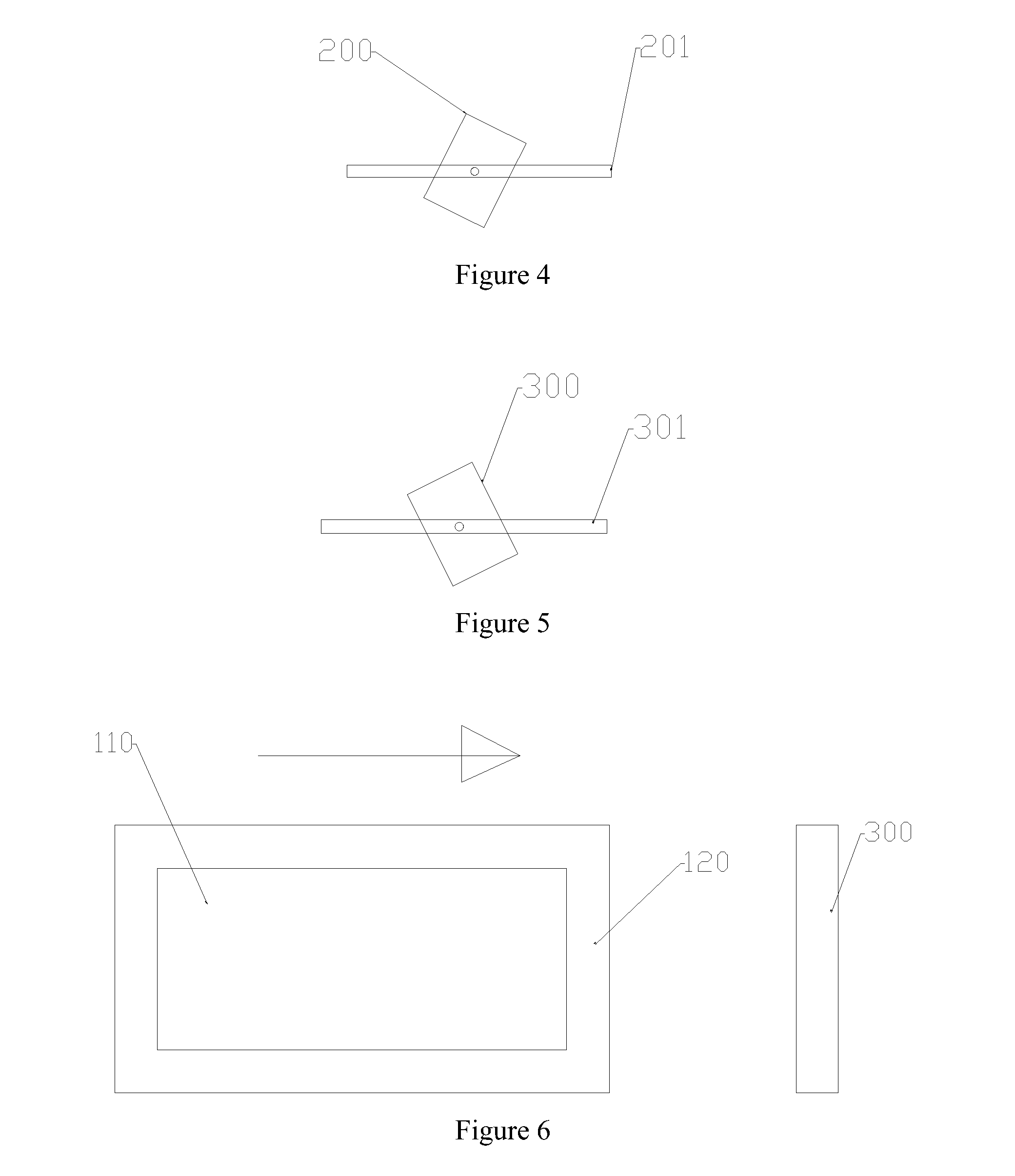
[0034]The substrate 100, such as the glass substrate used in the TFT-LCD, shown in FIGS. 1 and 2 is tested in the present invention. The front surface of the substrate 100 comprises a processing area 110 and a non-processing area 120. The processing area 110 is an area in which a semiconductor array is set. The non-processing area 120 is a area without printed circuit patterns. The non-processing area 120 is set around the processing area 110. Since the processing area 110 has a semiconductor array, the optical methods for testing the substrate can not be implemented on the processing area 110 effectively, for example, the photoelectric testing method and the pictorial testing method can not be implemented effectively.

[0035]However, in a common display substrate, the front surface is provided with a processing area 110 and a non-processing area ...


PUM


Abstract

A method and device for testing the quality of a display substrate are provided to detect whether the substrate has been broken. The device comprises an ultrasonic emitter and an ultrasonic receiver, both of which are set on the side opposite to the processing area, and it further comprises an ultrasonic analyzer connected to the ultrasonic receiver. The ultrasonic emitter emits ultrasonic waves for testing to the substrate, the ultrasonic receiver receives the ultrasonic waves reflected from the substrate, and the ultrasonic analyzer connected to the ultrasonic receive analyzes the received ultrasonic waves to determine whether the substrate has been broken. In the present invention, the fragment on anywhere comprising the processing area and the non-processing area of the substrate can be detected, the broken substrate can be picked out overall, and thus preventing the broken substrate from damaging the production line and the products.

Description

FIELD OF THE INVENTION[0001]The present invention relates to the field of manufacturing technology for substrate, and more particularly to a device and method for testing the quality of a display substrate.BACKGROUND OF THE INVENTION[0002]During the manufacturing process for the substrates such as TFT-LCDs, the test for the manufacturing quality of the substrate is demanded to find out whether there is fragment in the substrate. In traditional manufacturing technology, the fragment is sought mainly through a photoelectric testing method or a pictorial testing method.[0003]In the photoelectric testing method, a light emitting device can emit light to the substrate to be tested, and then a light sensor can receive the light reflected from the substrate, whether the substrate has been broken can be determined by testing the change of the intensity of the reflected light. However, this kind of testing method will be influenced by the manufacturing process of the substrate. Since the pro...

Claims


Application Information

Patent Timeline
IPC IPC(8): G01N29/04
CPCG01N29/041G01N29/265G01N2291/0231
Inventor LI, LIANGREN, BOYANG
Owner SHENZHEN CHINA STAR OPTOELECTRONICS TECH CO LTD
Why Eureka
Try Eureka