Statistical model-based metrology

Active Publication Date: 2014-10-02
KLA TENCOR CORP
View PDF1 Cites 160 Cited by
  • Summary
  • Abstract
  • Description
  • Claims
  • Application Information

AI Technical Summary

Benefits of technology

The patent text describes a measurement model that can receive directly measurement data and provide process parameter values or structure parameter values as output. This streamlining process improves predictive results and reduces computation and user time. The model can measure process parameters even when the underlying structure topology is changing due to process variations. The use of multiple targets or measurement techniques can increase the sample and process information embedded in the model and enable more accurate measurements. Overall, the measurement model enhances the accuracy and efficiency of the modeling process.

Problems solved by technology

As devices (e.g., logic and memory devices) move toward smaller nanometer-scale dimensions, characterization becomes more difficult.
Devices incorporating complex three-dimensional geometry and materials with diverse physical properties contribute to characterization difficulty.
For example, modern memory structures are often high-aspect ratio, three-dimensional structures that make it difficult for optical radiation to penetrate to the bottom layers.
As a result, the measurement model parameters characterizing the target often cannot be reliably decoupled.
In response to these challenges, more complex optical tools have been developed.
In addition, the spreading of light intensity over large wavelength ranges decreases illumination intensity at any particular wavelength and increases signal uncertainty of measurements performed at that wavelength.
Each step introduces errors and consumes a significant amount of computational and user time.
Typically, a model building task requires days, or even weeks, to complete.
In addition, the size of the library and the computation time associated with performing regression calculations during measurement reduces the throughput of the measurement system.
Future metrology applications present challenges for metrology due to increasingly small resolution requirements, multi-parameter correlation, increasingly complex geometric structures, and increasing use of opaque materials.

Method used


Image

  • Statistical model-based metrology
  • Statistical model-based metrology
  • Statistical model-based metrology

Examples


Embodiment Construction

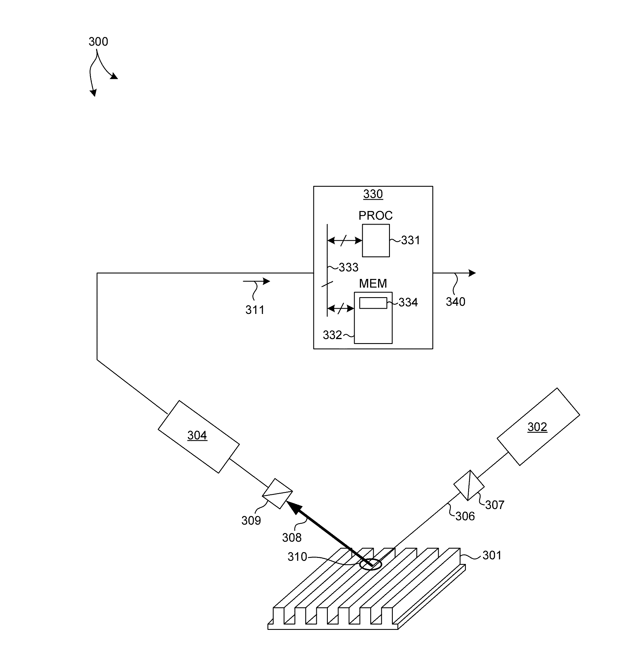
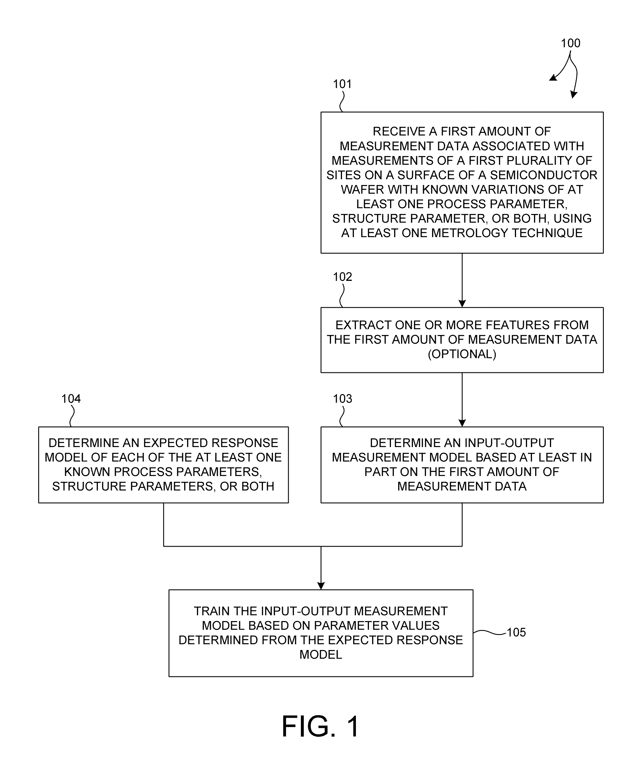
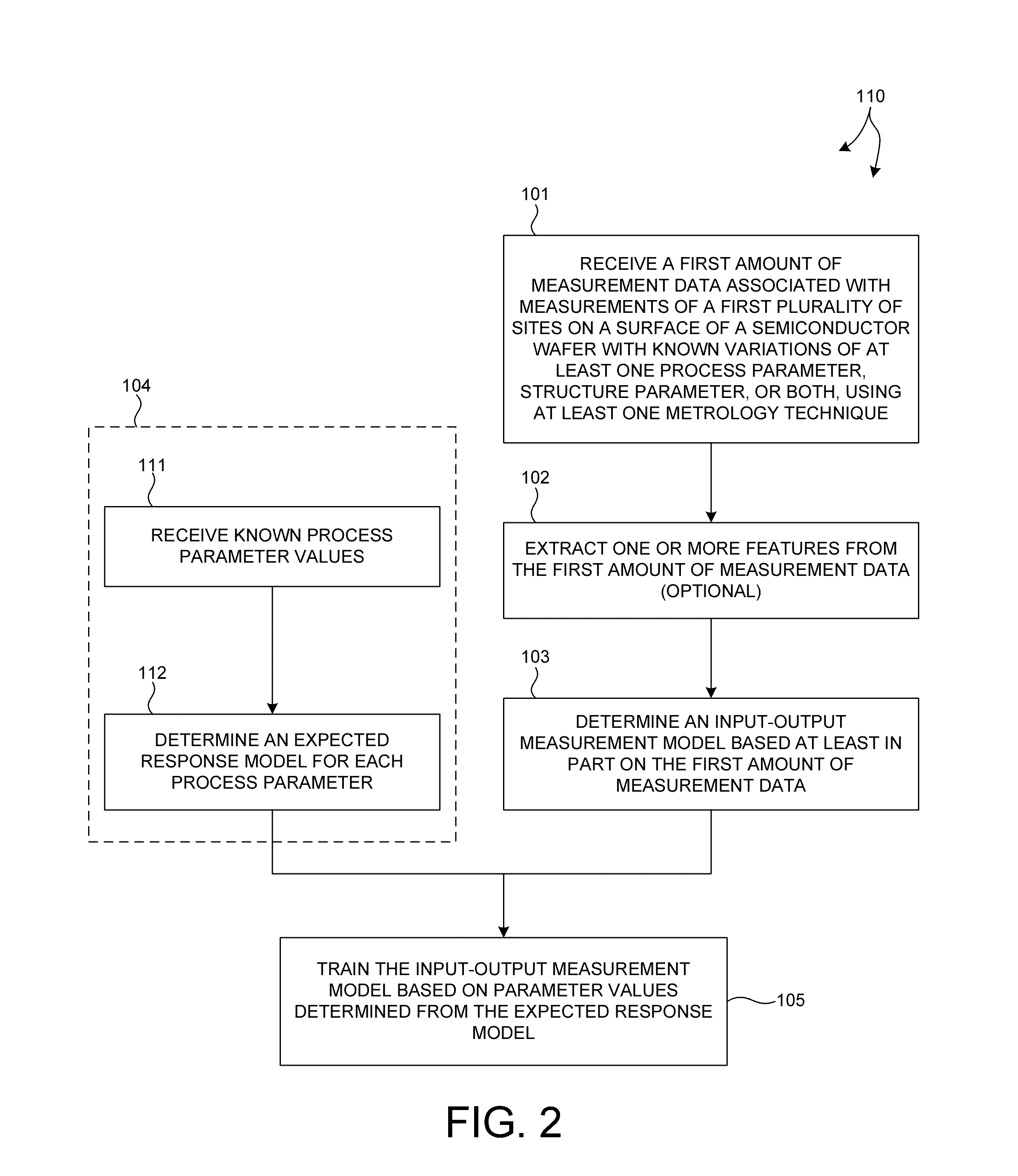
[0031]Reference will now be made in detail to background examples and some embodiments of the invention, examples of which are illustrated in the accompanying drawings.

[0032]Methods and systems for creating a measurement model based only on measured training data (e.g., spectra collected from a Design of Experiments (DOE) wafer) are presented. The trained measurement model is then used to calculate process parameter values, structure parameter values, or both, directly from measured data (e.g., spectra) collected from other wafers.

[0033]In one aspect, the measurement models described herein receive measurement data (e.g., measured spectra) directly as input and provide process parameter values, structure parameter values, or both, as output. By streamlining the modeling process, the predictive results are improved along with a reduction in computation and user time.

[0034]In a further aspect, process parameters are directly measured based on the measurement model created from raw mea...


PUM


Abstract

Methods and systems for creating a measurement model based on measured training data are presented. The trained measurement model is used to calculate process parameter values, structure parameter values, or both, directly from measured data collected from other wafers. The measurement models receive measurement data directly as input and provide process parameter values, structure parameter values, or both, as output. The measurement model enables the direct measurement of process parameters. Measurement data from multiple targets is collected for model building, training, and measurement. In some examples, the use of measurement data associated with multiple targets eliminates, or significantly reduces, the effect of under layers in the measurement result, and enables more accurate measurements. Measurement data collected for model building, training, and measurement, may be derived from measurements performed by a combination of multiple, different measurement techniques.

Description

CROSS REFERENCE TO RELATED APPLICATION[0001]The present application for patent claims priority under 35 U.S.C. §119 from U.S. provisional patent application Ser. No. 61 / 805,831, entitled “Optical Metrology Using Statistical Models for Direct Measurement of Structure and Process Parameters,” filed Mar. 27, 2013, the subject matter of which is incorporated herein by reference in its entirety.TECHNICAL FIELD[0002]The described embodiments relate to metrology systems and methods, and more particularly to methods and systems for improved parameter measurement.BACKGROUND INFORMATION[0003]Semiconductor devices such as logic and memory devices are typically fabricated by a sequence of processing steps applied to a specimen. The various features and multiple structural levels of the semiconductor devices are formed by these processing steps. For example, lithography among others is one semiconductor fabrication process that involves generating a pattern on a semiconductor wafer. Additional e...

Claims


Application Information

Patent Timeline
IPC IPC(8): H01L21/66
CPCH01L22/10H01L2924/0002G03F7/70641H01L22/12H01L22/20G03F7/70558H01L2924/00
Inventor PANDEV, STILIAN IVANOVMADSEN, JONATHAN M.
Owner KLA TENCOR CORP
Why Eureka
Try Eureka