Structure of MEMS electroacoustic transducer
a technology of electroacoustic transducers and electroacoustic transducers, which is applied in the direction of electromechanical transducers, semiconductor electrostatic transducers, diaphragms of transducers, etc., can solve the problems of difficult control of the quality of the polymer layer, unsatisfactory sensitivity of the electroacoustic transducer, etc., to improve the sensitivity of the mems electroacoustic transducer, easy integration
- Summary
- Abstract
- Description
- Claims
- Application Information
AI Technical Summary
Benefits of technology
Problems solved by technology
Method used
Image
Examples
first embodiment
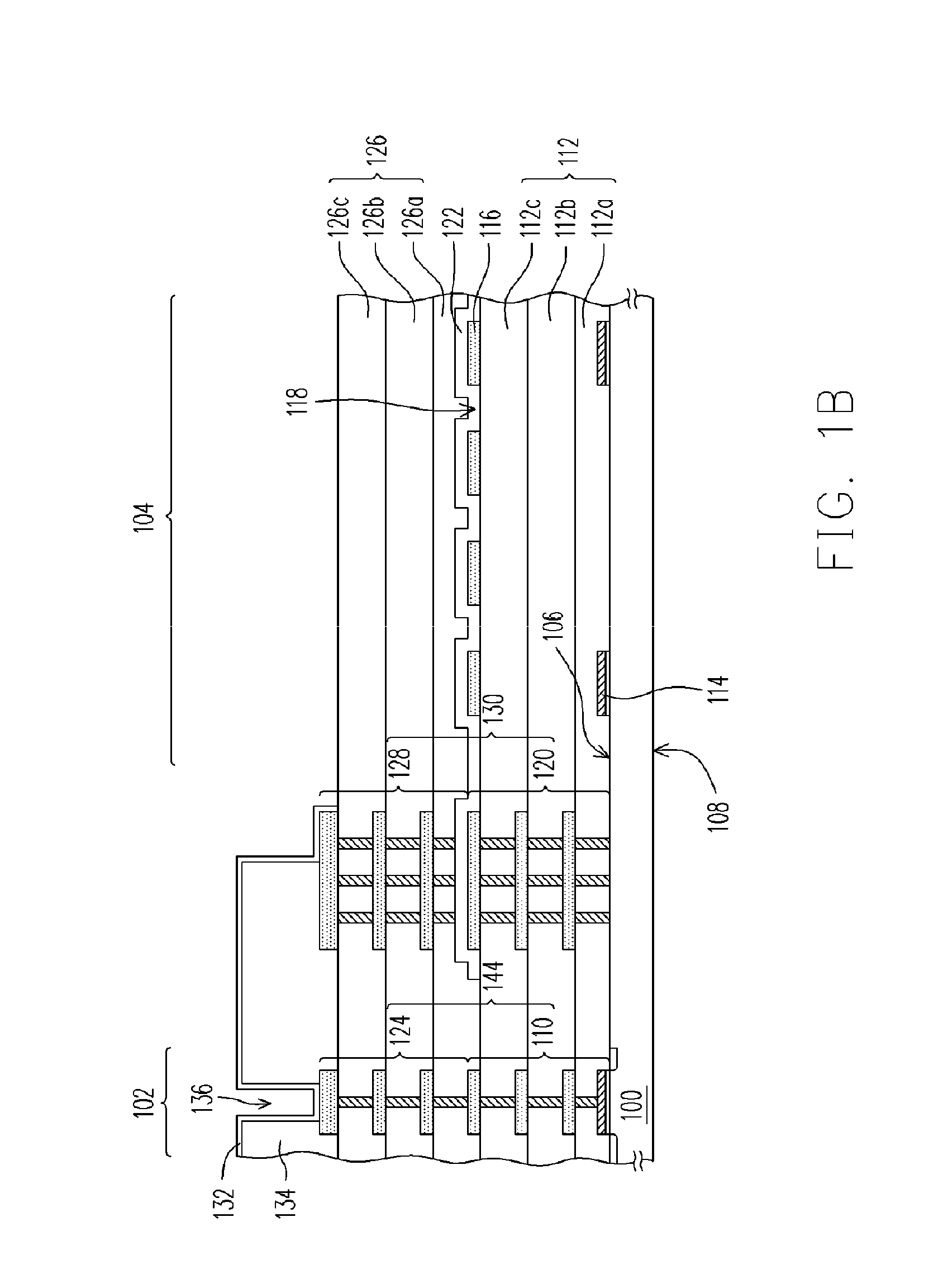
[0038]FIGS. 1A to 1D are cross-sectional views illustrating processes of fabricating a structure of micro-electro-mechanical systems (MEMS) electroacoustic transducer according to the present invention.
[0039]First, referring to FIG. 1A, a substrate 100 is provided. The substrate 100 includes a circuit region 102 and an MEMS device region 104. The substrate 100 has a front side 106 and a back side 108. The substrate 100 is, for example, a silicon substrate. Wherein, one of the ordinary skill in the art could modulate the disposition relationship between the circuit region 102 and the MEMS device region 104 depended on demand. For example, the MEMS device region 104 is located at the right side of the circuit region 102 in the first embodiment. In other embodiment, the MEMS device region 104 may be located at the left side of the circuit region 102.
[0040]Then, a metal interconnect structure 110 is formed on the front side 106 of the substrate 100 in the circuit region 102. The fabrica...
second embodiment
[0058]FIGS. 2A to 2C are cross-sectional views illustrating processes of fabricating a structure of MEMS electroacoustic transducer according to the present invention.
[0059]First, referring to FIGS. 2A, a substrate 200 is provided. The substrate 200 includes a circuit region 202, an MEMS device region 204, and a vent hole region 206. The substrate 200 is, for example, a silicon substrate. Wherein, one of the ordinary skill in the art could modulate the disposition relationship among the circuit region 202, the MEMS device region 204 and the vent hole region 206 depended on demand. For example, the circuit region 202 is located at one side of the MEMS device region 204, and the vent hole region 206 is located at the other side of the MEMS device region 204 in the second embodiment. In other embodiment, the circuit region 202 may be located at one side of the vent hole region 206, and the MEMS device region 204 may be located at the other side of the vent hole region 206.
[0060]Then, a...
PUM
 Abstract
Description
Claims
Application Information
 - R&D
- Intellectual Property
- Life Sciences
- Materials
- Tech Scout
- Unparalleled Data Quality
- Higher Quality Content
- 60% Fewer Hallucinations
Browse by: Latest US Patents, China's latest patents, Technical Efficacy Thesaurus, Application Domain, Technology Topic, Popular Technical Reports.
© 2025 PatSnap. All rights reserved.Legal|Privacy policy|Modern Slavery Act Transparency Statement|Sitemap|About US| Contact US: help@patsnap.com


