Metal card and manufacturing method thereof
- Summary
- Abstract
- Description
- Claims
- Application Information
AI Technical Summary
Benefits of technology
Problems solved by technology
Method used
Image
Examples
Example
First Embodiment
[0032]
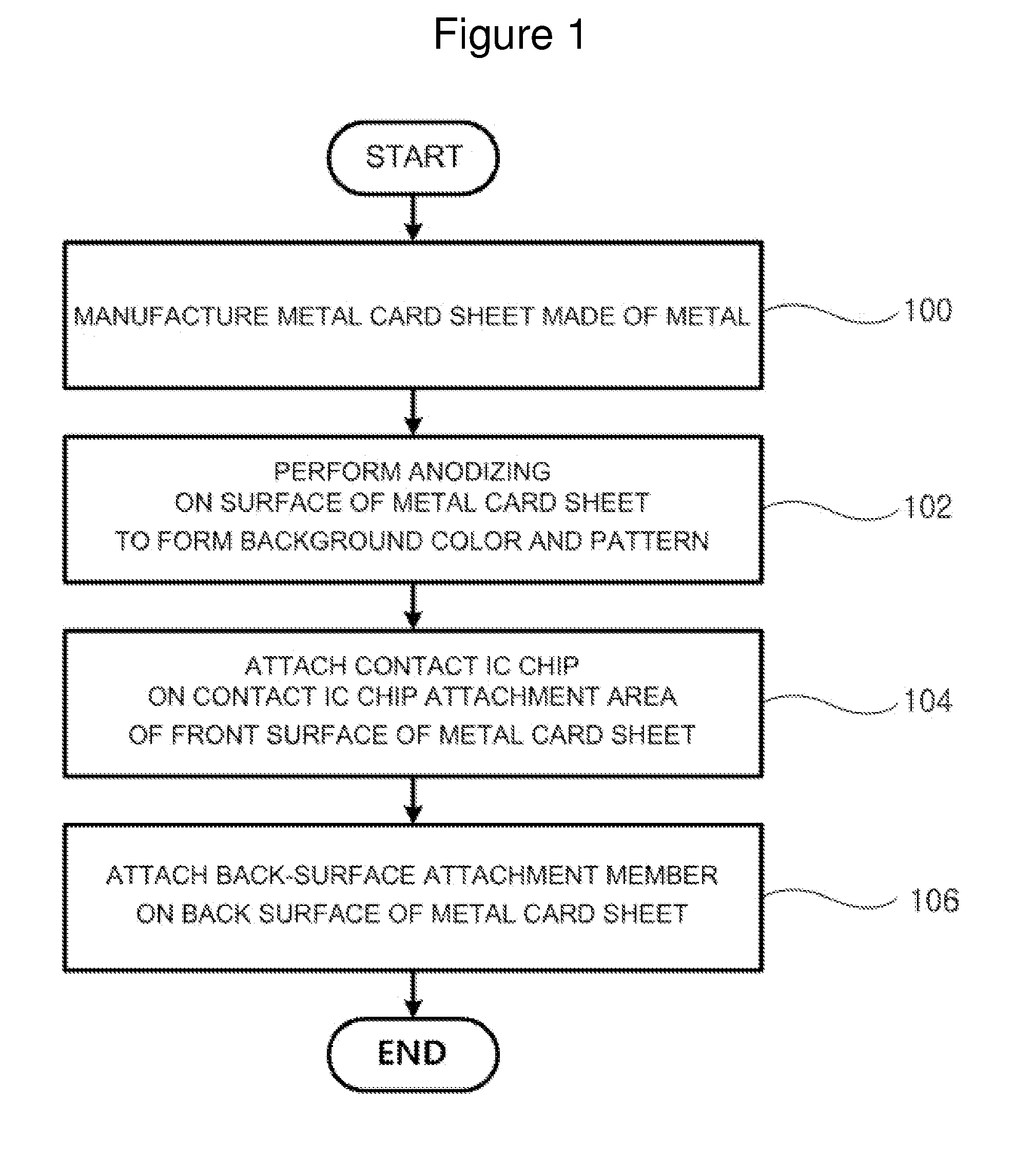
[0033]Referring to FIG. 1 illustrating a metal card manufacturing process according to a first embodiment of the present invention in brief, first, a duralumin metal card sheet is manufactured in order to manufacture a metal card (Step 100).
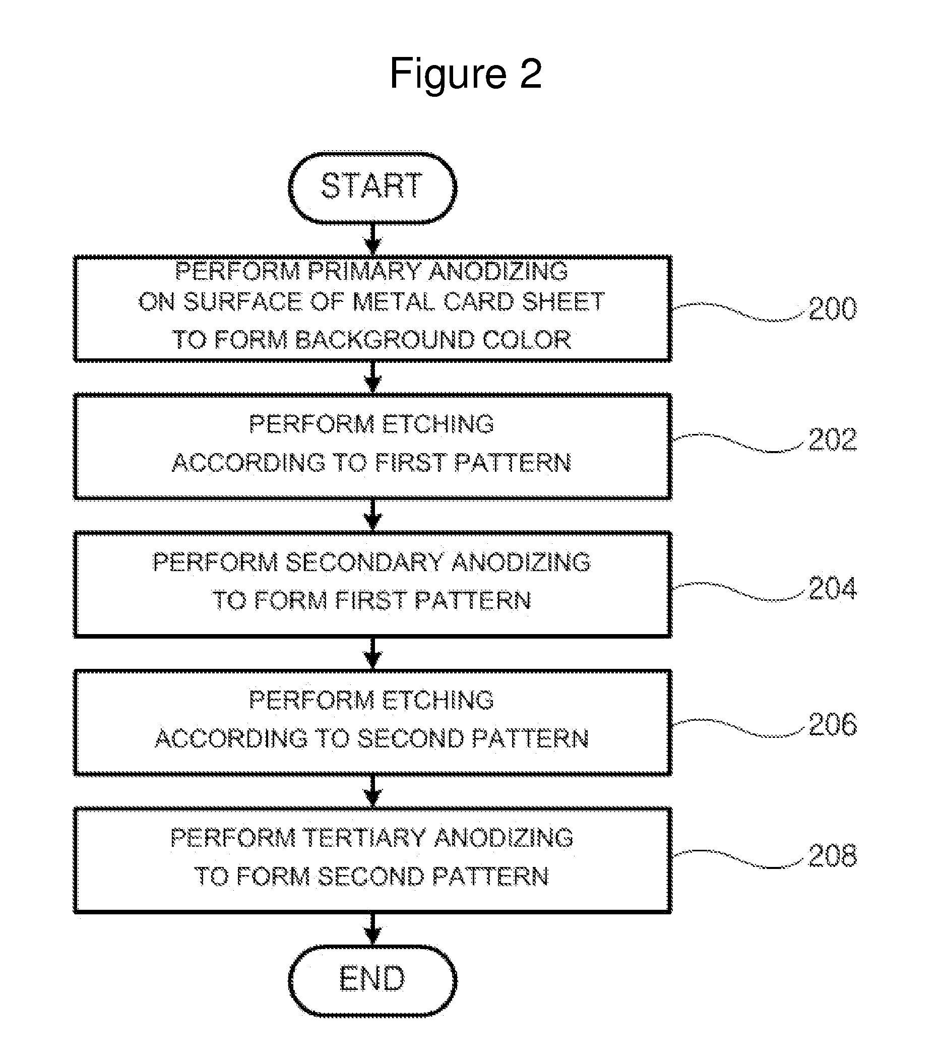
[0034]An anodized layer is formed by performing multiple times of anodizing and etching on a surface of the duralumin metal card sheet so as to form a background color and pattern and insulate the surface of the metal card sheet (Step 102).
[0035]A contact IC chip attachment area is formed on the front surface of the metal card sheet on which the background color and pattern are formed, and a contact IC chip is attached on the contact IC chip attachment area (Step 104).
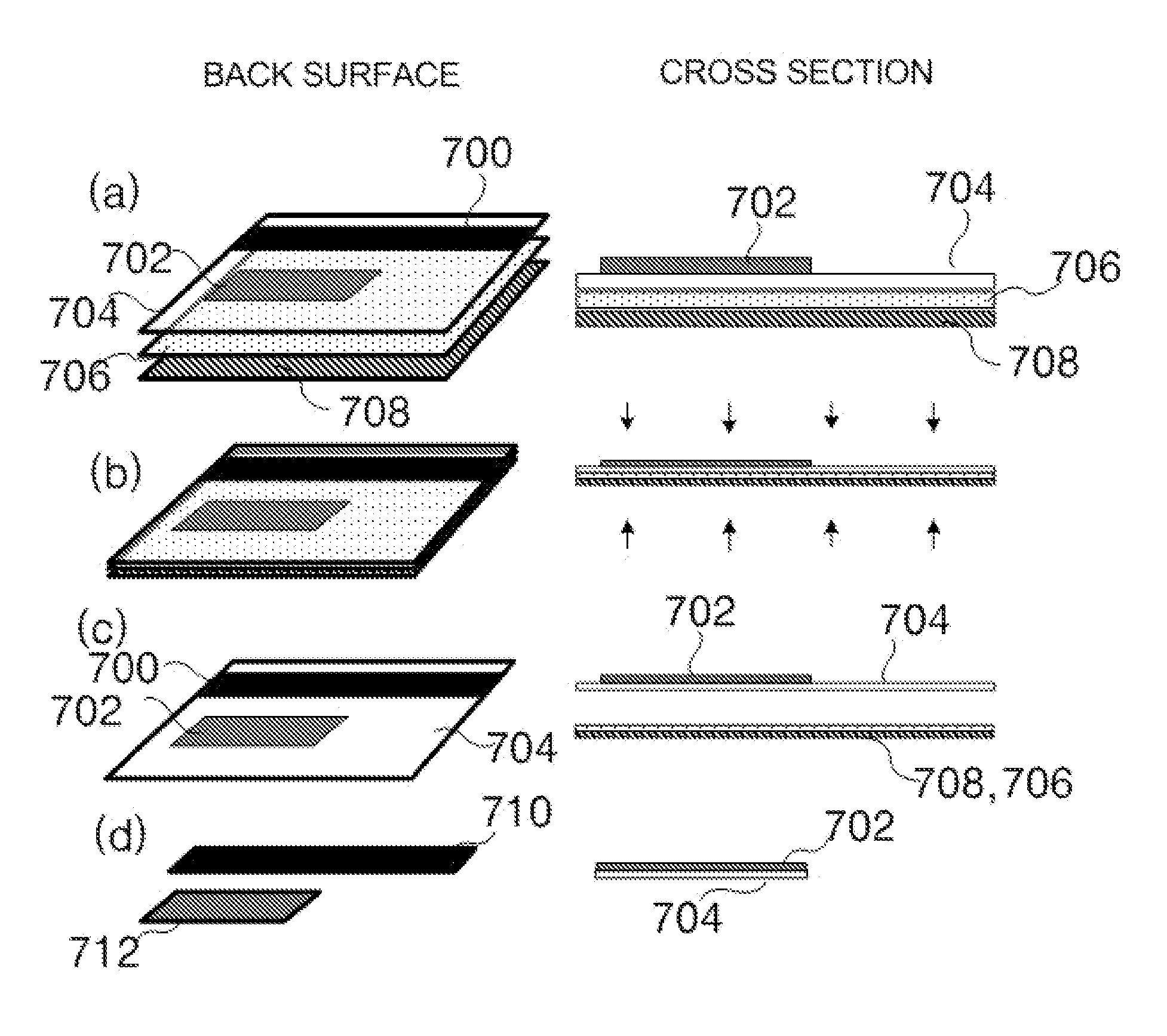
[0036]Next, magnetic-film attachment area and signature-plate attachment area are formed on the back surface of the metal card sheet, and a back-surface attachment member such as a magnetic film and a signature plate is attached on the magnetic-film and signatu...
Example
Second Embodiment
[0091]
[0092]Referring to FIG. 15 illustrating a metal card manufacturing process according to a second embodiment of the present invention, first, a duralumin metal card sheet is manufactured in order to manufacture a metal card (Step c00).
[0093]An area having a step shape having a size and depth capable of receiving a contact IC chip is formed on a front surface of a metal card sheet by performing etching on an area on which the contact IC chip is attached (Step c02). An anodized layer is formed by performing multiple times of anodizing and etching on the surface of the duralumin metal card sheet and the step-shaped etched area, so that a background color and pattern are formed and the surface of the metal card sheet is insulated (Step c04).
[0094]On the front surface of the metal card sheet on which the background color and pattern are formed, after the etched area is applied with an adhesive resin, the contact IC chip is inserted, and after that, thermal pressing ...
PUM
| Property | Measurement | Unit |
|---|---|---|
| Area | aaaaa | aaaaa |
Abstract
Description
Claims
Application Information
 - R&D
- Intellectual Property
- Life Sciences
- Materials
- Tech Scout
- Unparalleled Data Quality
- Higher Quality Content
- 60% Fewer Hallucinations
Browse by: Latest US Patents, China's latest patents, Technical Efficacy Thesaurus, Application Domain, Technology Topic, Popular Technical Reports.
© 2025 PatSnap. All rights reserved.Legal|Privacy policy|Modern Slavery Act Transparency Statement|Sitemap|About US| Contact US: help@patsnap.com


