
Lateral bipolar junction transistor

a lateral bipolar junction and transistor technology, applied in the field of cmos-based lateral bipolar junction transistors, can solve the problems of reducing the size and the optimization of the performance of the cmos and the bipolar device is considered a significant challenge, and achieves the effect of high beta

Active Publication Date: 2014-05-08
MEDIATEK INC
View PDF3 Cites 58 Cited by
  • Summary
  • Abstract
  • Description
  • Claims
  • Application Information

AI Technical Summary

Benefits of technology

This patent describes a method for making a lateral bipolar junction transistor (BJT) with high beta. The method involves using a block layer to mask a portion of the substrate and then performing a threshold voltage implant process. The block layer is removed and a gate is formed over the substrate. The transistor includes an emitter region, a base region, a collector region, and a salicide layer. The technical effect of this patent is that it describes a way to increase the beta of BJTs making them better suited for certain applications.

Problems solved by technology

However, there is considerable challenge in optimizing the performance of both CMOS and bipolar devices fabricated with progressively reduced dimensions.

Method used


Image

  • Lateral bipolar junction transistor
  • Lateral bipolar junction transistor
  • Lateral bipolar junction transistor

Examples


Embodiment Construction

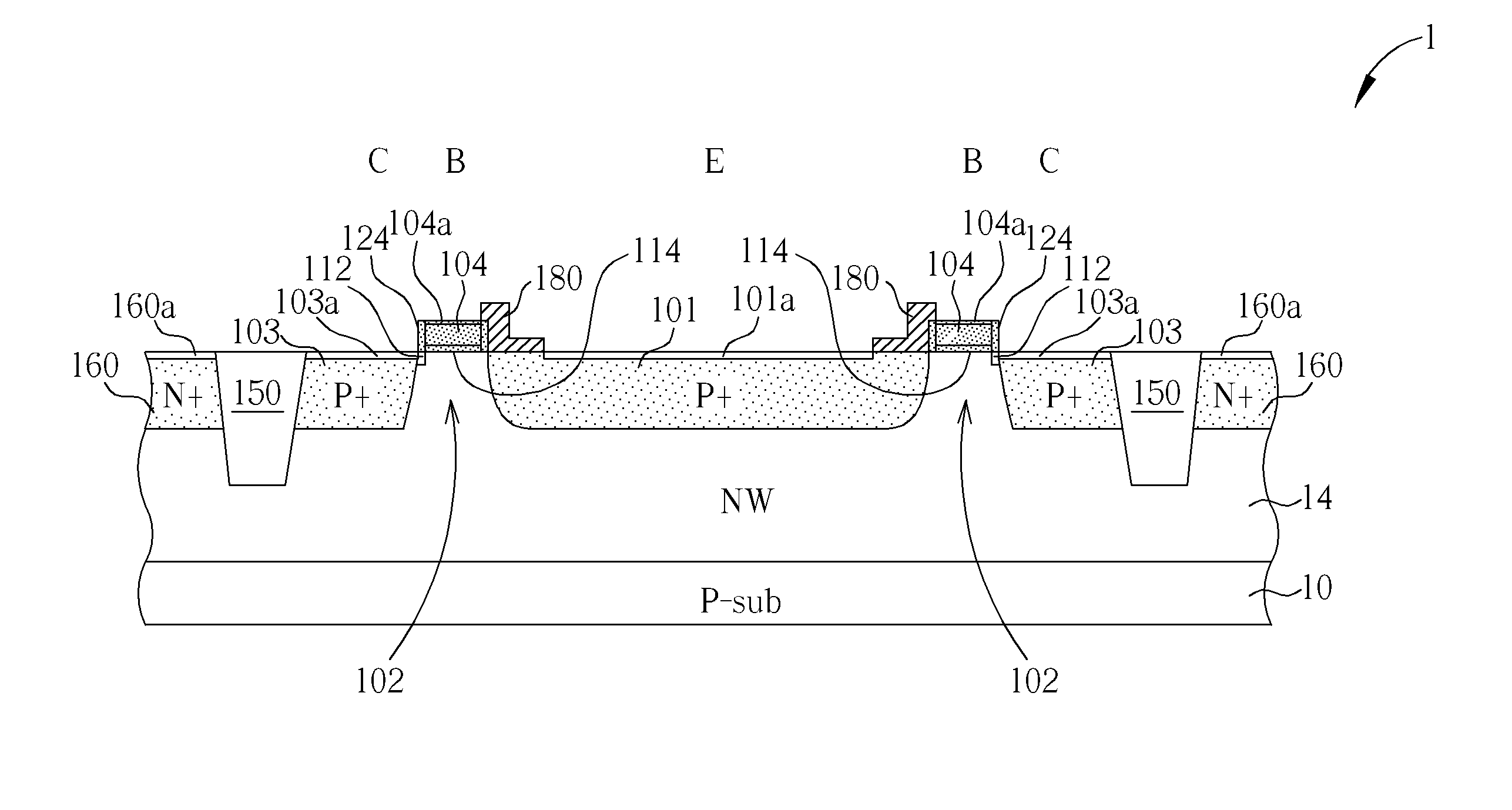
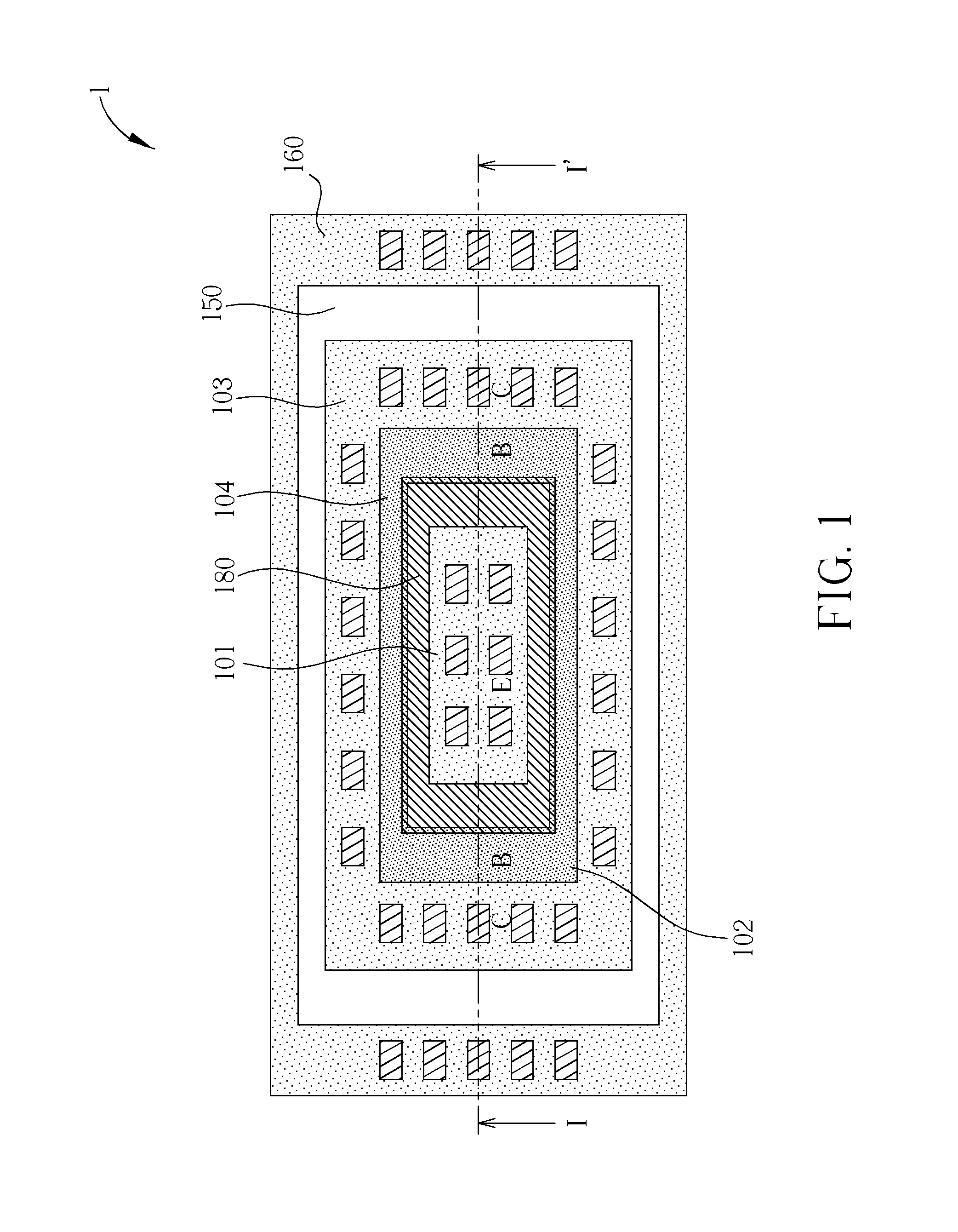
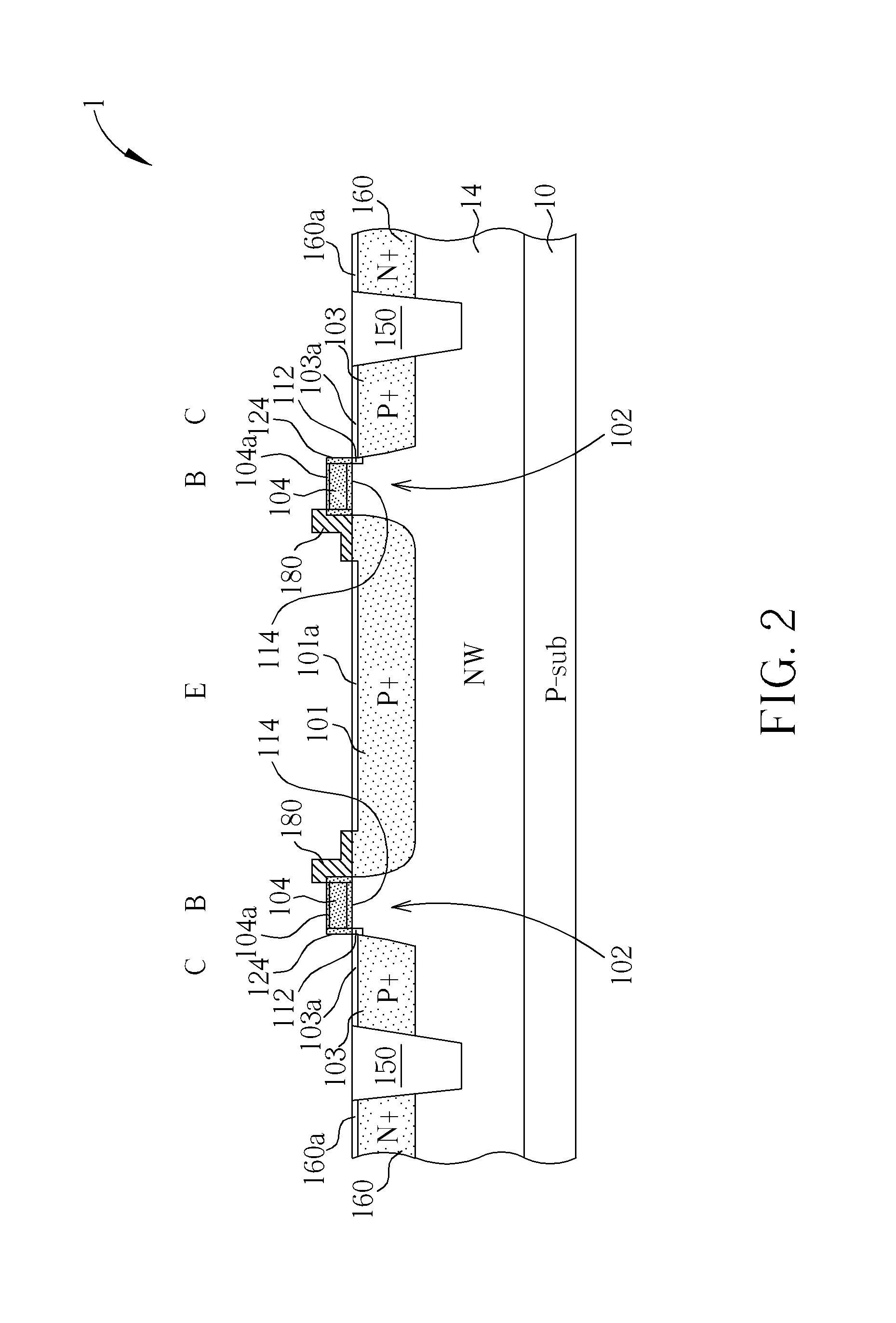
[0018]The structure and layout of the present invention lateral bipolar junction transistor (LBJT) with higher current gain are described in detail. The improved LBJT structure is described for a lateral PNP bipolar transistor, but it should be understood by those skilled in the art that by reversing the polarity of the conductive dopants lateral NPN bipolar transistors can be made.

[0019]Please refer to FIG. 1 and FIG. 2. FIG. 1 is a top planar view of a layout of the substantially concentric lateral bipolar transistor according to one embodiment of the invention. FIG. 2 is a schematic, cross-sectional view of the transistor in FIG. 1, taken along line I-I′ of FIG. 1. As shown in FIG. 1 and FIG. 2, the lateral PNP bipolar transistor 1 is formed in a semiconductor substrate 10 such as a P type doped silicon substrate. The lateral PNP bipolar transistor 1 comprises a P+ doping region 101 that functions as an emitter region of the lateral PNP bipolar transistor 1, which is formed withi...


PUM


Abstract

A lateral bipolar junction transistor includes an emitter region; a base region surrounding the emitter region; a gate disposed at least over a portion of the base region; and a collector region surrounding the base region; wherein the portion of the base region under the gate does not under go a threshold voltage implant process.

Description

CROSS REFERENCE TO RELATED APPLICATIONS[0001]This application is a continuation of U.S. application Ser. No. 12 / 389,378 filed Feb. 20, 2009, which is included in its entirety herein by reference.BACKGROUND OF THE INVENTION[0002]1. Field of the Invention[0003]The invention relates to the field of semiconductor technology and, more particularly, to a CMOS-based lateral bipolar junction transistor (lateral BJT) with high beta.[0004]2. Description of the Prior Art[0005]Bipolar junction transistors or bipolar transistors, which are formed using a CMOS compatible process, are well known in the art. These bipolar transistors are also referred to as lateral bipolar junction transistors and have high threshold frequency (Ft) and high beta.[0006]In the design of semiconductor integrated circuits, it is often desirable to provide a mixed mode device, i.e., which has both BJT and CMOS functions. Mixed mode devices both increase the flexibility of the IC design and increase the performance of th...

Claims


Application Information

Patent Timeline
Patent Type & Authority Applications(United States)
IPC IPC(8): H01L27/06
CPCH01L27/0623H01L21/8249H01L29/0649H01L29/0692H01L29/0821H01L29/6625H01L29/735
Inventor KO, CHING-CHUNGLEE, TUNG-HSING
Owner MEDIATEK INC
Learn More