Low image sticking OLED display

a low-level, image-sticking technology, applied in the direction of discharge tube luminescnet screens, discharge tube/lamp details, electric discharge lamps, etc., can solve the problems of reducing the deposition area of fmm beyond its original design, affecting the performance of blue sub-pixels, and affecting the performance of organic light-emitting devices. , to achieve the effect of improving the performance of organic light-emitting devices, reducing the degree of image sticking, and improving the performance of blue sub-

Active Publication Date: 2014-03-20
UNIVERSAL DISPLAY
View PDF0 Cites 29 Cited by
  • Summary
  • Abstract
  • Description
  • Claims
  • Application Information

AI Technical Summary

Benefits of technology

[0024]Devices and techniques are provided to improve the performance of organic light emitting devices and, more spe

Problems solved by technology

However the FMM requires a far tighter alignment tolerance (e.g. on the order of the dimension of a portion of the sub-pixels) and thereby usually takes longer to align, which may add significantly to the time and cost of manufacturing.
This can cause problems in the display ar

Method used


Image

  • Low image sticking OLED display
  • Low image sticking OLED display
  • Low image sticking OLED display

Examples


Embodiment Construction

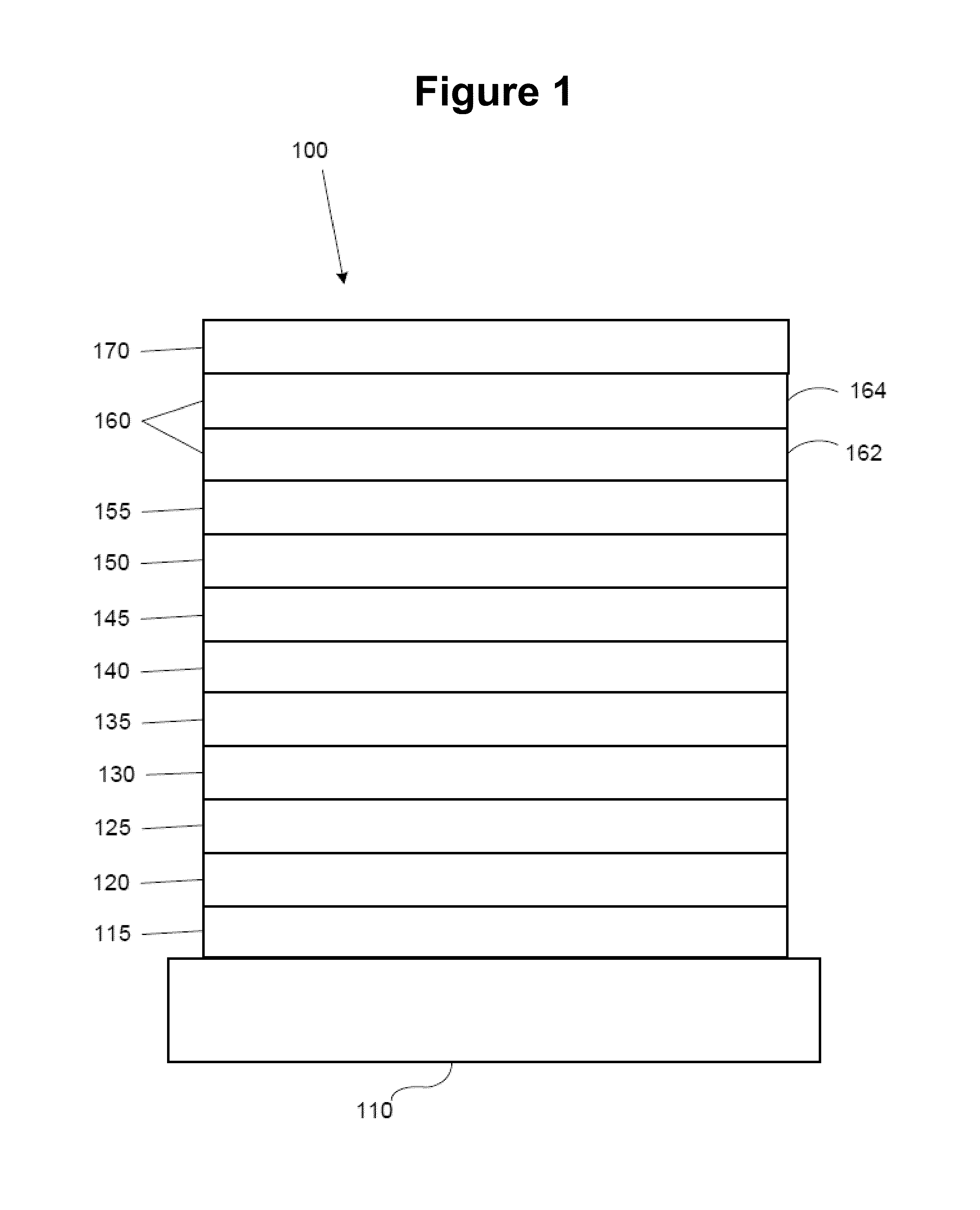
[0050]Generally, an OLED comprises at least one organic layer disposed between and electrically connected to an anode and a cathode. When a current is applied, the anode injects holes and the cathode injects electrons into the organic layer(s). The injected holes and electrons each migrate toward the oppositely charged electrode. When an electron and hole localize on the same molecule, an “exciton,” which is a localized electron-hole pair having an excited energy state, is formed. Light is emitted when the exciton relaxes via a photoemissive mechanism. In some cases, the exciton may be localized on an excimer or an exciplex. Non-radiative mechanisms, such as thermal relaxation, may also occur, but are generally considered undesirable.

[0051]The initial OLEDs used emissive molecules that emitted light from their singlet states (“fluorescence”) as disclosed, for example, in U.S. Pat. No. 4,769,292, which is incorporated by reference in its entirety. Fluorescent emission generally occur...


PUM


Abstract

Devices and fabrication methods thereof are provided which reduce image sticking and/or improve lifetime and performance of blue emissive devices. Each device may include non-common transport layers between emissive devices, one or more optical capping layers, light and deep blue emissive devices, a mixed host emissive layer, a high T1 transport layer, and/or a stacked blue device in conjunction with single emissive layer red and/or green devices. The provided structures may be used individually, in combination, or as a group in a single device.

Description

[0001]The claimed invention was made by, on behalf of and / or in connection with one or more of the following parties to a joint university corporation research agreement: Regents of the University of Michigan, Princeton University, The University of Southern California, and the Universal Display Corporation. The agreement was in effect on and before the date the claimed invention was made, and the claimed invention was made as a result of activities undertaken within the scope of the agreement.FIELD OF THE INVENTION[0002]The present invention relates to light emitting devices and, more specifically, to OLEDs with improved performance, especially with regard to the degree of image sticking exhibited by the device.BACKGROUND[0003]Opto-electronic devices that make use of organic materials are becoming increasingly desirable for a number of reasons. Many of the materials used to make such devices are relatively inexpensive, so organic opto-electronic devices have the potential for cost ...

Claims


Application Information

Patent Timeline
IPC IPC(8): H05B33/14
CPCH10K59/32H10K59/351H10K59/352H10K50/11H10K2101/40H10K2101/10H10K2101/90H10K2101/30
Inventor WEAVER, MICHAEL STUARTHACK, MICHAELBROWN, JULIA J.PREMUTICO, MAURO
Owner UNIVERSAL DISPLAY
Why Eureka
Try Eureka