Light emitting diode and method of manufacturing the same
a technology of light-emitting diodes and manufacturing methods, which is applied in the direction of semiconductor/solid-state device manufacturing, electrical apparatus, semiconductor devices, etc., can solve the problems of limited flexibility, ito film, and wavelength-dependent transmittance variation, and achieve the effect of improving light-emitting efficiency
Inactive Publication Date: 2013-10-31
GWANGJU INST OF SCI & TECH
View PDF16 Cites 13 Cited by
- Summary
- Abstract
- Description
- Claims
- Application Information
AI Technical Summary
Benefits of technology
[0011]Therefore, the present invention is aimed at providing a light emitting diode, which includes a graphene film having metal nanopartic
Problems solved by technology
However, the ITO film has problems such as transmittance variation according to wavelength, limited flexibility, depletion of indium as a raw material thereof, and the like.
However, since graphene consists of carbon atoms bonded to each other, it exhibits low adhesion to an inorganic material layer when applied to an inorganic material-based light emitting diode, so that some of the graphene film is lost in a transfer process and causes deterioration in luminescent characteristics.
In addition, since the graphene film has a very low thickness, so
Method used
View moreImage
Smart ImageViewing Examples

Examples
 PUM
 Abstract
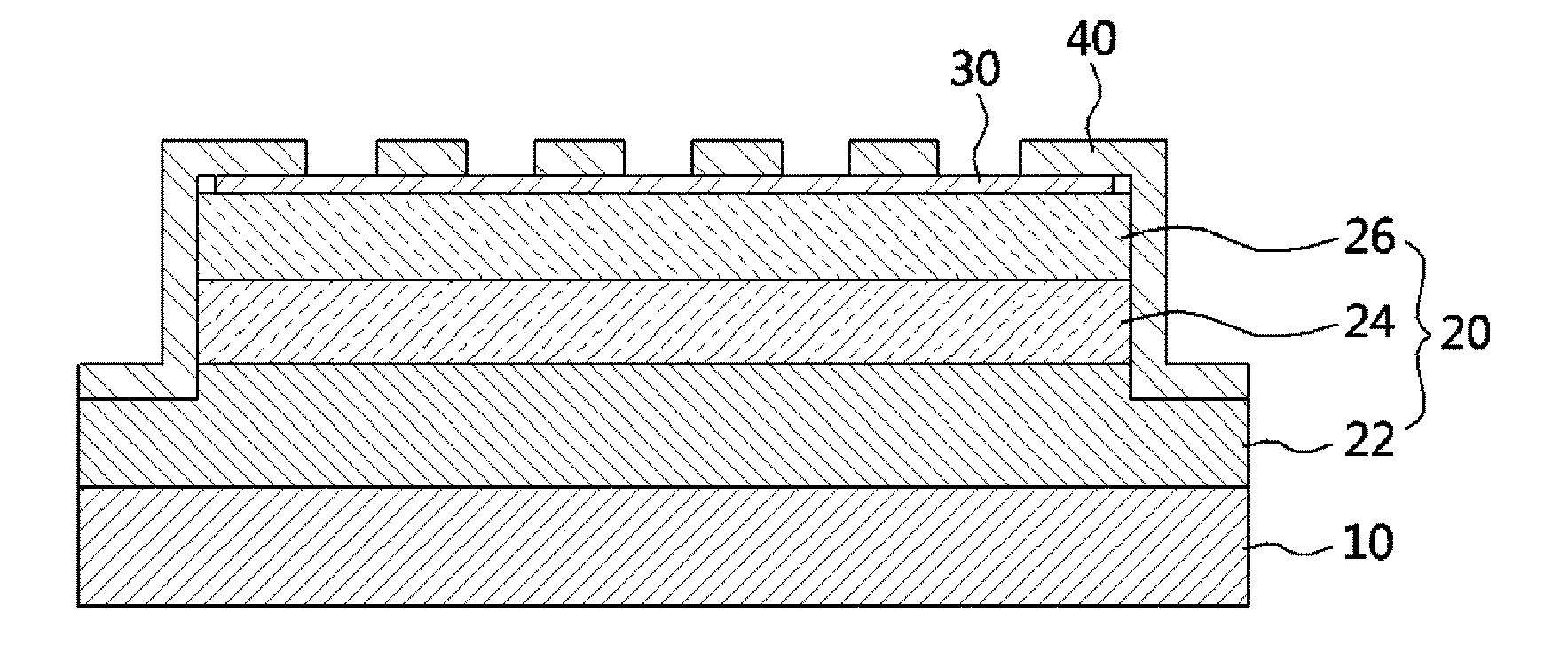
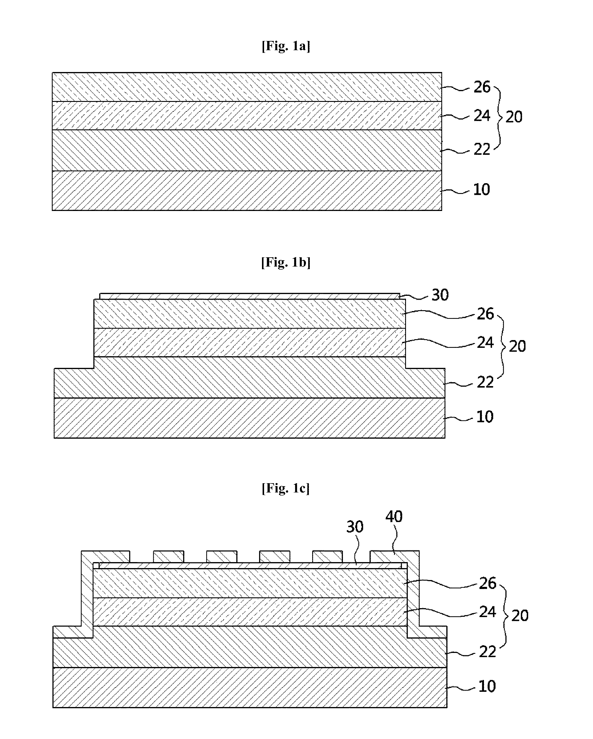
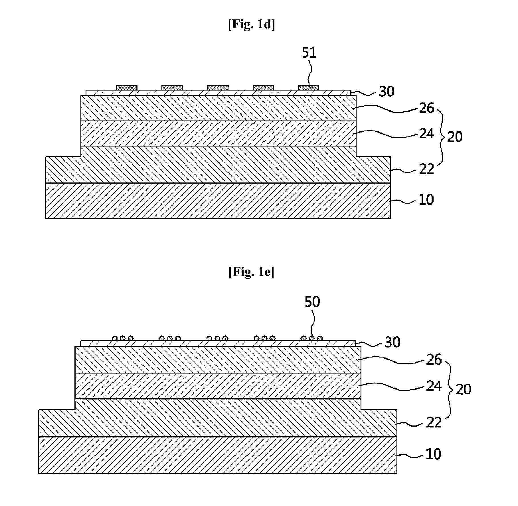
The present disclosure provides a light emitting diode and a method of manufacturing the same. The light emitting diode includes a graphene layer on a second conductive semiconductor layer and a plurality of metal nanoparticles formed on some region of the graphene layer, whereby adhesion between the second conductive semiconductor layer comprised of an inorganic material and the graphene layer is enhanced, thereby securing stability and reliability of the light emitting diode. In addition, the light emitting diode allows uniform spreading of electric current, thereby allowing stable emission of light through a surface area of the light emitting diode. The method of manufacturing a light emitting diode includes forming a graphene layer on a second conductive semiconductor layer, forming a mask film on the graphene layer, forming a metal layer within the patterns of the mask film, followed by removing the mask film; and heat treating the metal layer to form a plurality of metal nanoparticles, whereby the metal nanoparticles having a high index of refraction are formed on some region of the graphene layer and provide surface texturing effects, thereby improving light emission efficiency.
Description
CROSS-REFERENCE TO RELATED APPLICATION[0001]This application claims priority to Korean Patent Application No. 10-2012-0044091 filed on 26 Apr. 2012 and all the benefits accruing therefrom under 35 U.S.C. §119, the contents of which are incorporated by reference in their entirety.BACKGROUND[0002]1. Technical Field[0003]The present invention relates to a light emitting diode and a method of manufacturing the same, and more particularly, to an inorganic material-based light emitting diode, which uses graphene as a current spreading layer, and a method of manufacturing the same.[0004]2. Description of the Related Art[0005]Currently, an indium tin oxide (ITO) film obtained by doping tin oxide into indium oxide is most commonly used as a current spreading layer of a light emitting diode. However, the ITO film has problems such as transmittance variation according to wavelength, limited flexibility, depletion of indium as a raw material thereof, and the like. Thus, various studies have bee...
Claims
Login to View More Application Information
Patent Timeline
 IPC IPC(8): H01L33/04
CPCH01L33/04H01L33/42H01L33/40H01L33/38
Inventor LEE, DONG SEONSHIM, JAE PHILPARK, SEONG JUCHOE, MIN HYEOKKIM, DO HYUNGLEE, TAK HEE
Owner GWANGJU INST OF SCI & TECH
Features
- R&D
- Intellectual Property
- Life Sciences
- Materials
- Tech Scout
- Unparalleled Data Quality
- Higher Quality Content
- 60% Fewer Hallucinations
Learn More Browse by: Latest US Patents, China's latest patents, Technical Efficacy Thesaurus, Application Domain, Technology Topic, Popular Technical Reports.
© 2025 PatSnap. All rights reserved.Legal|Privacy policy|Modern Slavery Act Transparency Statement|Sitemap|About US| Contact US: help@patsnap.com