Optoelectronic device for differential photoreception, with automatic compensation of phase and amplitude imbalances

Inactive Publication Date: 2013-08-08
ALCATEL LUCENT SAS
View PDF4 Cites 0 Cited by
  • Summary
  • Abstract
  • Description
  • Claims
  • Application Information

AI Technical Summary

Benefits of technology

The patent text describes a solution for improving the reception performance of optoelectronic devices that use differential signaling. These devices often have imbalances between the two complementary signals, which can degrade their performance. The solution involves using a balanced photodetector and a differential amplification process to automatically compensate for the imbalances. This can reduce the need for costly components and fabrication processes and improve the ultimate performance of the device. The optoelectronic device can also include additional features such as phase and amplitude adjustments and a phase and amplitude error detector to further enhance its performance.

Problems solved by technology

However, the components that are combined to produce these optoelectronic devices and the fabrication processes of these components and optoelectronic devices often introduce imperfections causing imbalances between the two complementary signals before they are subtracted, thus degrading the reception performance.
Since typically no imbalance compensation can be realized by these optoelectronic devices, specific and demanding characteristics may be required for the components and fabrication processes involving the components in which differential signaling is used (for instance from the optical demodulator outputs that provide the two complementary optical signals to the photodetection means of the photoreceiver).
This may lead to costly components and fabrication processes.
Furthermore, whatever the quality of the components and fabrication processes, the optoelectronic devices may have remaining imperfections and possible characteristic shifts during their lifetime, and therefore the ultimate performance benefit that should bring the differential detection may become hard to achieve.

Method used


Image

  • Optoelectronic device for differential photoreception, with automatic compensation of phase and amplitude imbalances
  • Optoelectronic device for differential photoreception, with automatic compensation of phase and amplitude imbalances

Examples


Embodiment Construction

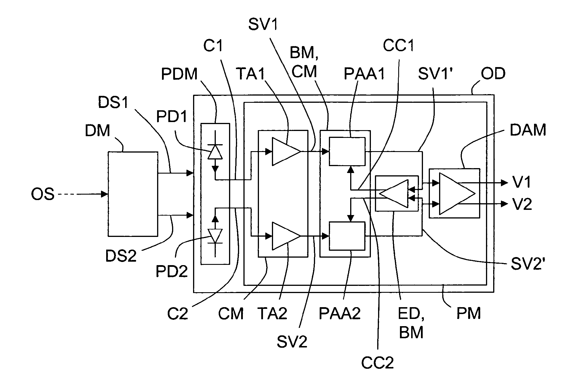
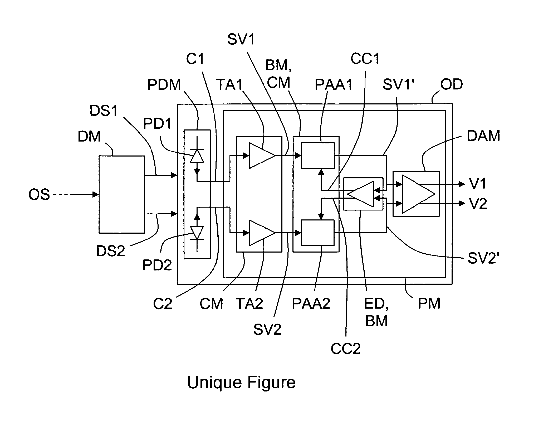
[0022]Embodiments of the invention aim at providing an optoelectronic device OD capable of automatically compensating for amplitude and phase imbalances.

[0023]In the following description, it will be considered, as example, that the optoelectronic device OD is a differential photoreceiver. But, the optoelectronic device OD could be also a device offering several functions and notably photoreception.

[0024]As illustrated in the unique FIGURE, an optoelectronic device OD, according to the invention, comprises at least a photodetection means PDM and a processing means PM.

[0025]The photodetection means PDM comprises first and second inputs which may be connected respectively to first and second outputs of an optical demodulator DM. The optical demodulator DM is arranged for demodulating each input optical signal it receives on its input to produce first DS1 and second DS2 optical complementary signals that it outputs onto its first and second outputs.

[0026]The photodetection means PDM ma...


PUM


Abstract

An optoelectronic device includes a photodetection means arranged for converting first and second complementary optical signals into first and second complementary currents, and a processing means arranged for processing these first and second complementary currents to output at least a first output voltage. This processing means includes i) a conversion means arranged for separately converting the first and second complementary currents into first and second operating voltages, ii) a balancing means arranged for balancing phase and amplitude of the first and second operating voltages, and iii) a differential amplification means arranged for applying a subtraction function to the first and second operating voltages with balanced phase and amplitude to produce at least the first output voltage, which is proportional to the difference between the first and second operating voltages with balanced phase and amplitude.

Description

[0001]The present invention relates to optoelectronics, and in particular to optoelectronic devices that offer at least a photoreception function or constitute photoreceivers.BACKGROUND ART[0002]As it is known by a person skilled in the art, in some technical domains, such as optical communication, differential signaling can be an efficient way of carrying information data with a better immunity to a certain number of parasitic signals. The information data is recovered by realizing a subtraction of two complementary signals, that need to be kept well balanced in phase and amplitude until the subtraction is realized.[0003]In the case of optical communications, these two complementary signals are typically generated by an optical component from one or several input optical signals. Then, an optoelectronic device may be used, which typically comprises a photodetection means arranged for converting the first and second complementary optical signals into first and second complementary c...

Claims


Application Information

Patent Timeline
IPC IPC(8): H04B10/06H04B10/66
CPCH04B10/6971H04B10/66
Inventor DUPUY, JEAN-YVESJORGE, FILIPEKONCZYKOWSKA, AGNIESZKA
Owner ALCATEL LUCENT SAS
Why Eureka
Try Eureka