System and method for reducing integrated circuit timing derating

Inactive Publication Date: 2013-06-13
AVAGO TECH WIRELESS IP SINGAPORE PTE
View PDF7 Cites 5 Cited by
  • Summary
  • Abstract
  • Description
  • Claims
  • Application Information

AI Technical Summary

Benefits of technology

This patent text describes a method and computer-readable storage medium for reducing timing derating in an integrated circuit design. The method involves extracting data about cells in a path and calculating a timing derating based on whether these cells are simple cells. This helps improve the performance of the circuit and ensure accurate timing.

Problems solved by technology

Signals that propagate too slowly through the circuit cause setup violations; signals that propagate too quickly through the circuit cause hold violations.
Setup or hold violations frustrate the logic of the circuit and prevent it from performing the job it was designed to do.

Method used


Image

  • System and method for reducing integrated circuit timing derating
  • System and method for reducing integrated circuit timing derating
  • System and method for reducing integrated circuit timing derating

Examples


Embodiment Construction

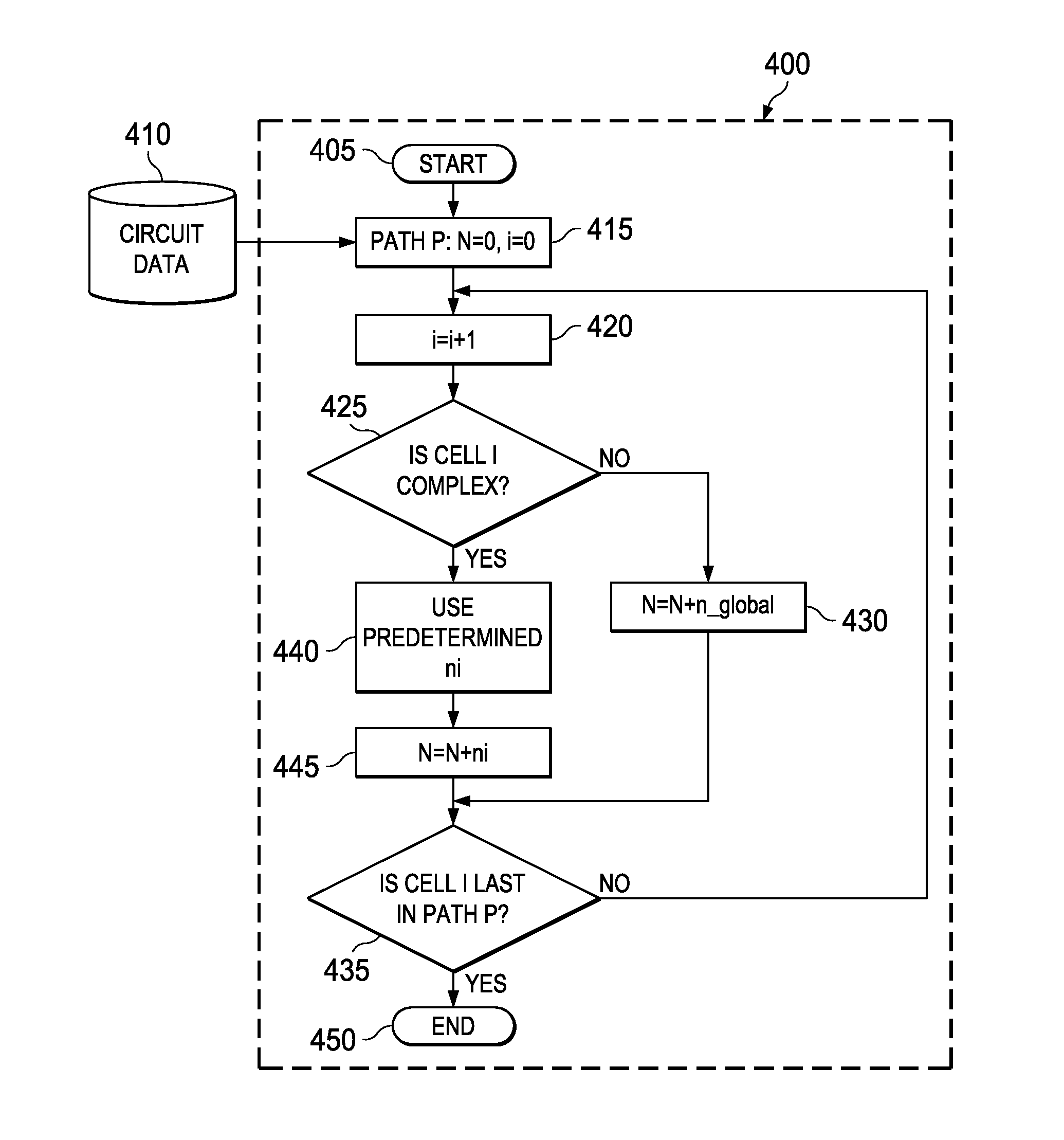
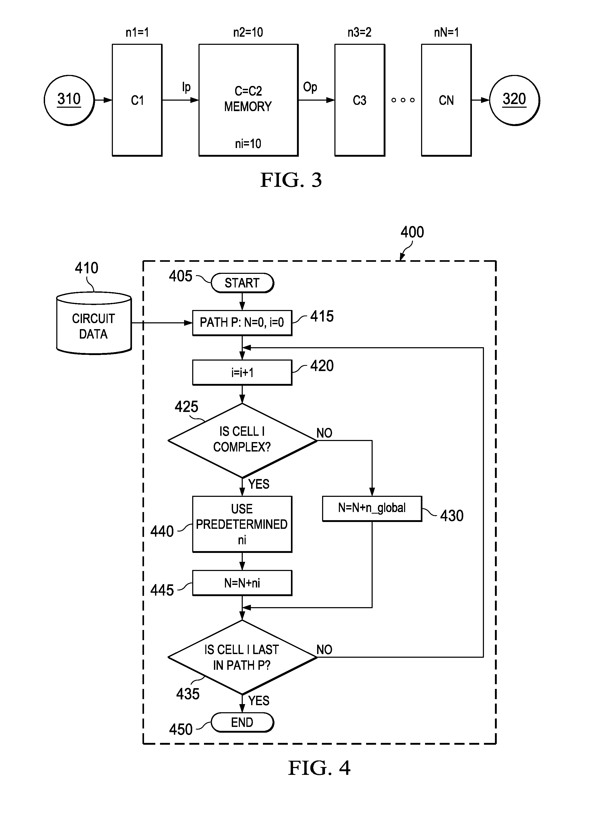
[0014]Described herein are various embodiments of a system and method for reducing the total timing derating that is to be applied to logical or clock paths of hierarchical designs or designs with complex cells during timing signoff to take OCV into account. Some embodiments of the system and method allow the total timing derating to be reduced to a minimum. Other embodiments reduce the timing derating that is to be applied to both logical and clock paths.

[0015]A relatively sophisticated but conventional process for determining timing derating and performing STA timing signoff is “Advanced OCV,” or AOCV, commercially available as part of the PrimeTime® system from Synopsys of Mountain View, Calif. AOCV assigns cell and net deratings as a function of a (logical) path depth N and a (physical) distance D of cells. Unfortunately, AOCV only analyzes paths down to the cell level. It does not take into account the internal logic depth (ni) of the cells themselves. Instead, AOCV globally (f...


PUM


Abstract

A system for, and method of, reducing IC timing derating for a path in an integrated circuit design. In one embodiment, the system includes an electronic design automation tool configured to (1) extract circuit data regarding cells in the path and (2) calculate a timing derating for the path based at least in part on a determination as to whether the cells are simple cells.

Description

TECHNICAL FIELD[0001]This application is directed, in general, to integrated circuit (IC) design and, more specifically, to a timing signoff system and method that takes static and dynamic voltage drop into account.BACKGROUND[0002]Circuit designers use electronic design automation (EDA) tools, a category of computer aided design (CAD) tools, to design and lay out electronic circuits, including simulating the operation of the circuit, determining where cells (i.e., logic elements including devices, e.g., transistors) should be placed and where the interconnects that couple the cells together should be routed. EDA tools allow designers to construct a circuit and simulate its performance using a computer and without requiring the costly and lengthy process of fabrication. EDA tools are indispensable for designing modern ICs, particularly very-large-scale integrated circuits (VSLICs). For this reason, EDA tools are in wide use.[0003]One such EDA tool performs timing signoff. Timing sign...

Claims


Application Information

Patent Timeline
IPC IPC(8): G06F17/50
CPCG06F17/5045G06F17/5031G06F30/3312G06F30/30G06F30/3315
Inventor TETELBAUM, ALEXANDER
Owner AVAGO TECH WIRELESS IP SINGAPORE PTE
Why Eureka
Try Eureka