Solid-state imaging device and imaging system

Active Publication Date: 2013-04-11
CANON KK
View PDF7 Cites 8 Cited by
  • Summary
  • Abstract
  • Description
  • Claims
  • Application Information

AI Technical Summary

Benefits of technology

The patent describes a type of camera sensor that can reduce the fixed noise in each column caused by the time delays between when different parts of the sensor report their results. As a result, the image quality is improved.

Problems solved by technology

Furthermore, the timing or temporal distances may not be scaled or depict the timing relationships in exact proportions.

Method used


Image

  • Solid-state imaging device and imaging system
  • Solid-state imaging device and imaging system
  • Solid-state imaging device and imaging system

Examples


Embodiment Construction

[0033]Various exemplary embodiments, features, and aspects of the disclosure will be described in detail below with reference to the drawings.

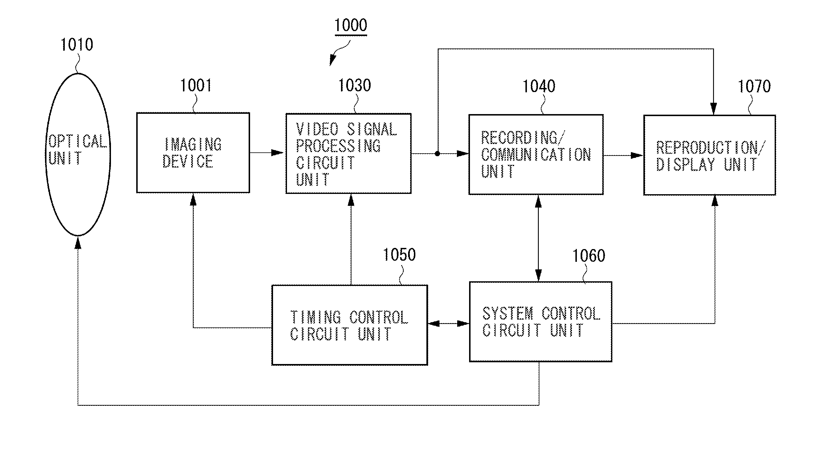
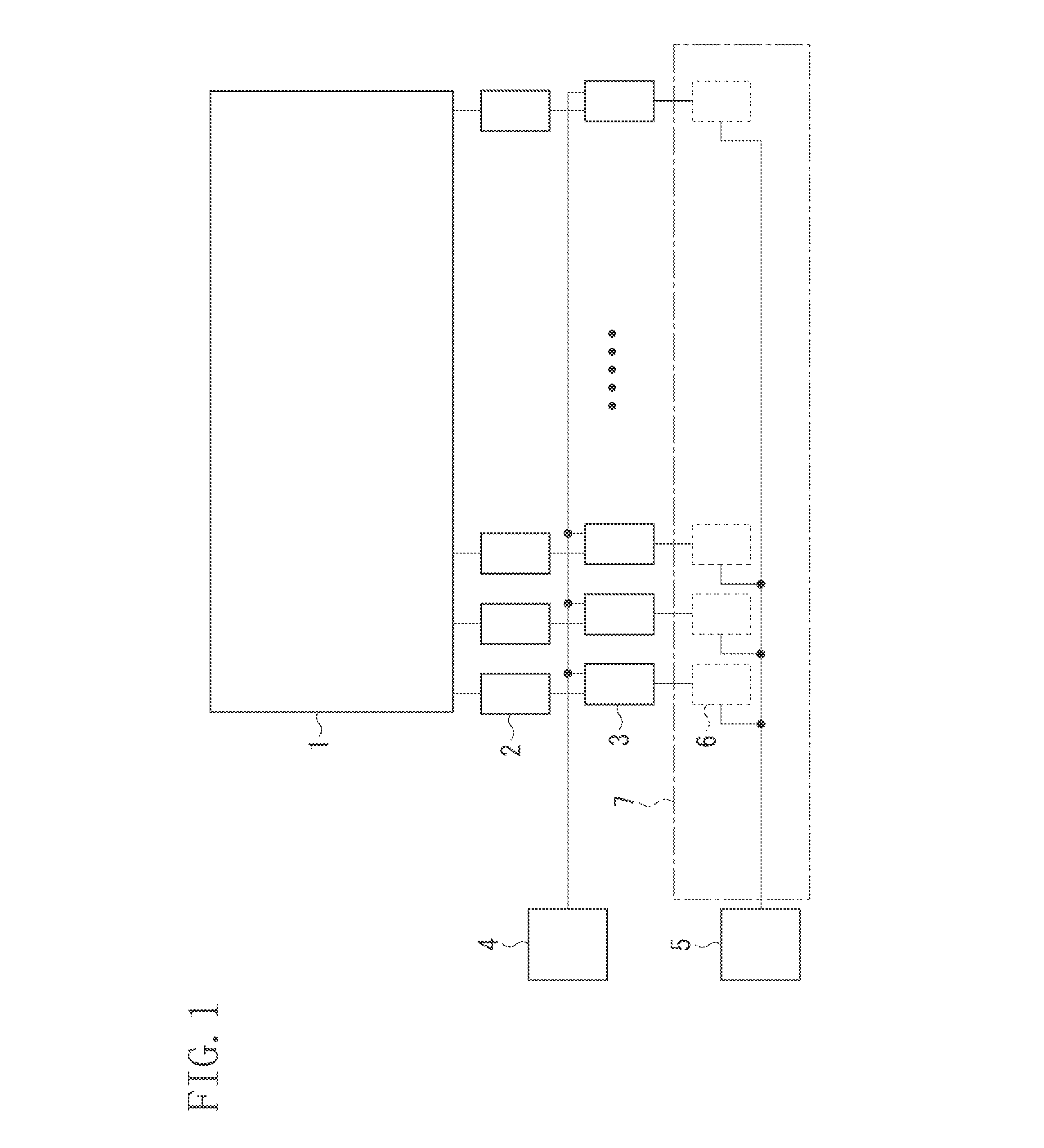
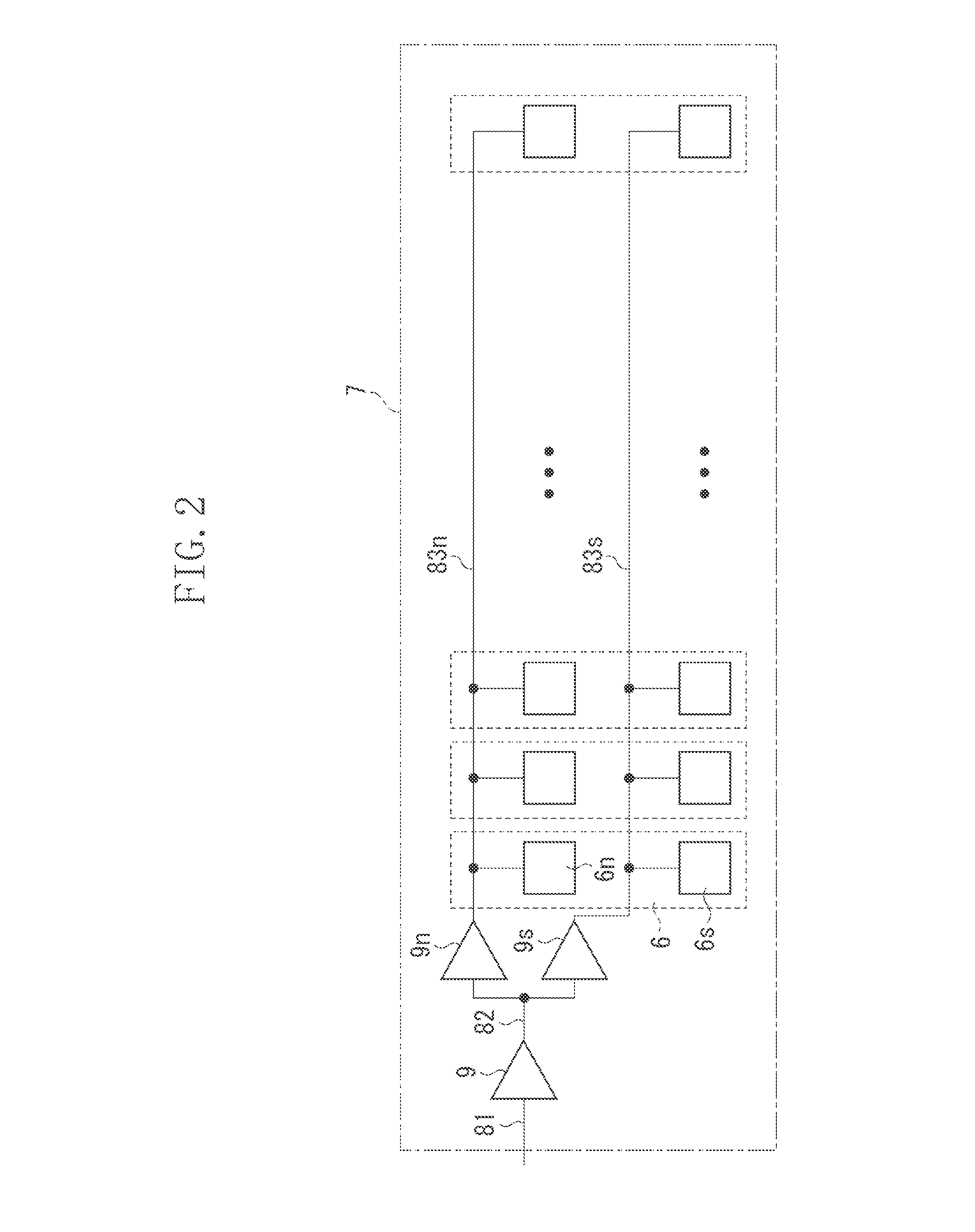
[0034]The first exemplary embodiment will be described below. FIG. 1 illustrates a configuration example of the solid-state imaging device according to the first exemplary embodiment. Referring to FIG. 1, the solid-state imaging device includes a pixel unit 1, a readout circuit 2, a comparison unit 3, a storing unit 6, a reference signal generation unit 4 which generates the reference signal, a counter 5, a horizontal scanning circuit, and a signal processing circuit. The readout circuit 2, the comparison unit 3, and the storing unit 6 are arranged in each column. The horizontal scanning circuit and the signal processing circuit will be described below with reference to FIG. 7.

[0035]The pixel unit 1 includes a plurality of pixels 210-1 arranged in a matrix, similarly as a pixel unit 210 illustrated in FIG. 7. The plurality of pixels 210-1 gene...


PUM


Abstract

A solid-state imaging device includes a plurality of pixels arranged in a matrix, a plurality of readout circuits provided in each column of the plurality of pixels arranged in a matrix, configured to read out for each column a signal of the plurality of pixels, a plurality of comparison units configured to compare a signal output from the plurality of readout circuits with a reference signal whose level changes with time, a counter configured to perform a count operation from when the level of the reference signal starts to change, first and second buffers each configured to buffer a count value of the counter, and a plurality of storing units connected to the plurality of comparison units, configured to store a count value of the counter when a magnitude relation between a signal output from the plurality of the readout circuits and the reference signal is inverted.

Description

BACKGROUND OF THE INVENTION[0001]1. Field of the Invention[0002]One disclosed aspect of the embodiments relates to a solid-state imaging device used in a scanner, a video camera, or a digital still camera.[0003]2. Description of the Related Art[0004]Recently, a complementary metal oxide semiconductor (CMOS) image sensor has been widely used in a digital camera, a digital video camera, or a camera unit in a cellular phone. Further, a CMOS image sensor which includes an analog-digital (AD) conversion circuit is in development in response to a demand to reduce the number of components and power consumption. An example of such a CMOS image sensor employs a column AD conversion circuit (ADC) technique in which an ADC is arranged in each column of a pixel array. A column ADC based on ramp architecture is a well-known type of the A / D conversion method used in the column ADC.[0005]The column ADC based on ramp architecture includes a comparator and a ramp signal source arranged in each colum...

Claims


Application Information

Patent Timeline
IPC IPC(8): H04N5/335
CPCH04N5/3658H04N5/76H04N5/378H04N25/677H04N25/75
Inventor ITANO, TETSUYAHIYAMA, HIROKISAITO, KAZUHIRONAKAMURA, KOHICHIIWATA, KOICHIROAKIYAMA, TAKESHIYAMAZAKIYOSHIDA, DAISUKE
Owner CANON KK
Why Eureka
Try Eureka