Conductive film with high transmittance having a number of anti reflection coatings, touch panel using the same and manufacturing method thereof
a technology of anti-reflection coating and conductive film, which is applied in the direction of conductive layers on insulating supports, instruments, coatings, etc., can solve the problems of failure to reach a commercially available transmittance, and achieve the effect of improving the transmittance of the ito film, reducing the refractive index and high refractivity
- Summary
- Abstract
- Description
- Claims
- Application Information
AI Technical Summary
Benefits of technology
Problems solved by technology
Method used
Image
Examples
second exemplary embodiment
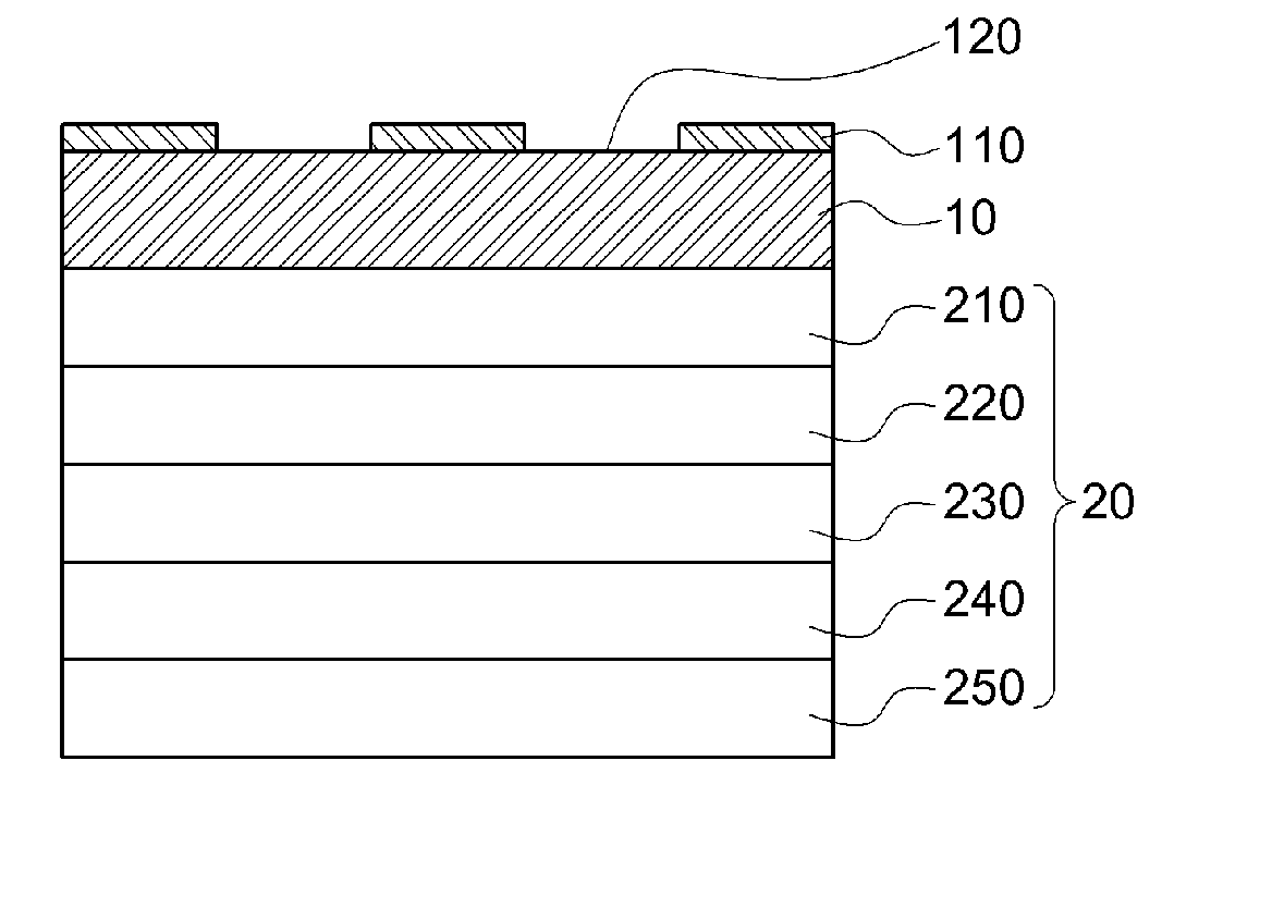
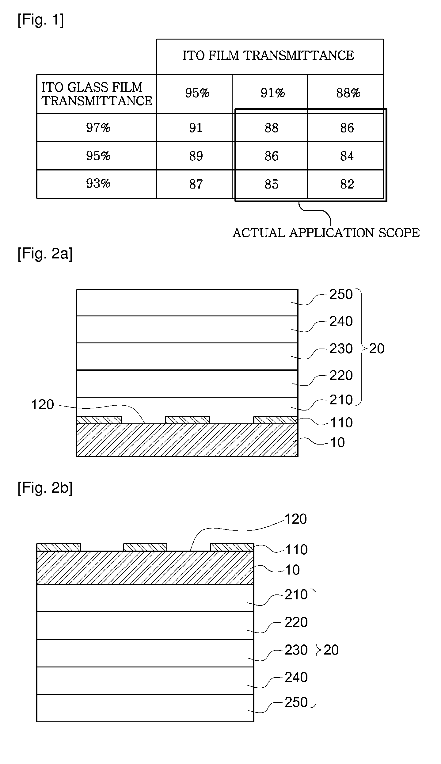
[0057]The second exemplary embodiment of the conductive film with a high transmittance and having a number of anti reflection coated films (20) includes, as shown in FIG. 2b, a conductive film (10) formed with a transparent electrode film pattern (110) and a number of AR films (20) coated in an opposite direction from that of the transparent electrode film pattern (110) on the conductive film (10).
[0058]As in the first exemplary embodiment, the number of anti reflection coated films (20) include a first layer film (210), a second layer film (220), a third layer film (230), a fourth layer film (240) and a fifth layer film (250), each sequentially formed from a surface contacting the conductive film (10) for preventing light reflection, where like reference numerals are used for like and corresponding films of the same layer.
[0059]In second exemplary embodiment, the number of anti reflection coated films (20) are formed on a rear surface of the conductive film (10) formed with the tra...
third exemplary embodiment
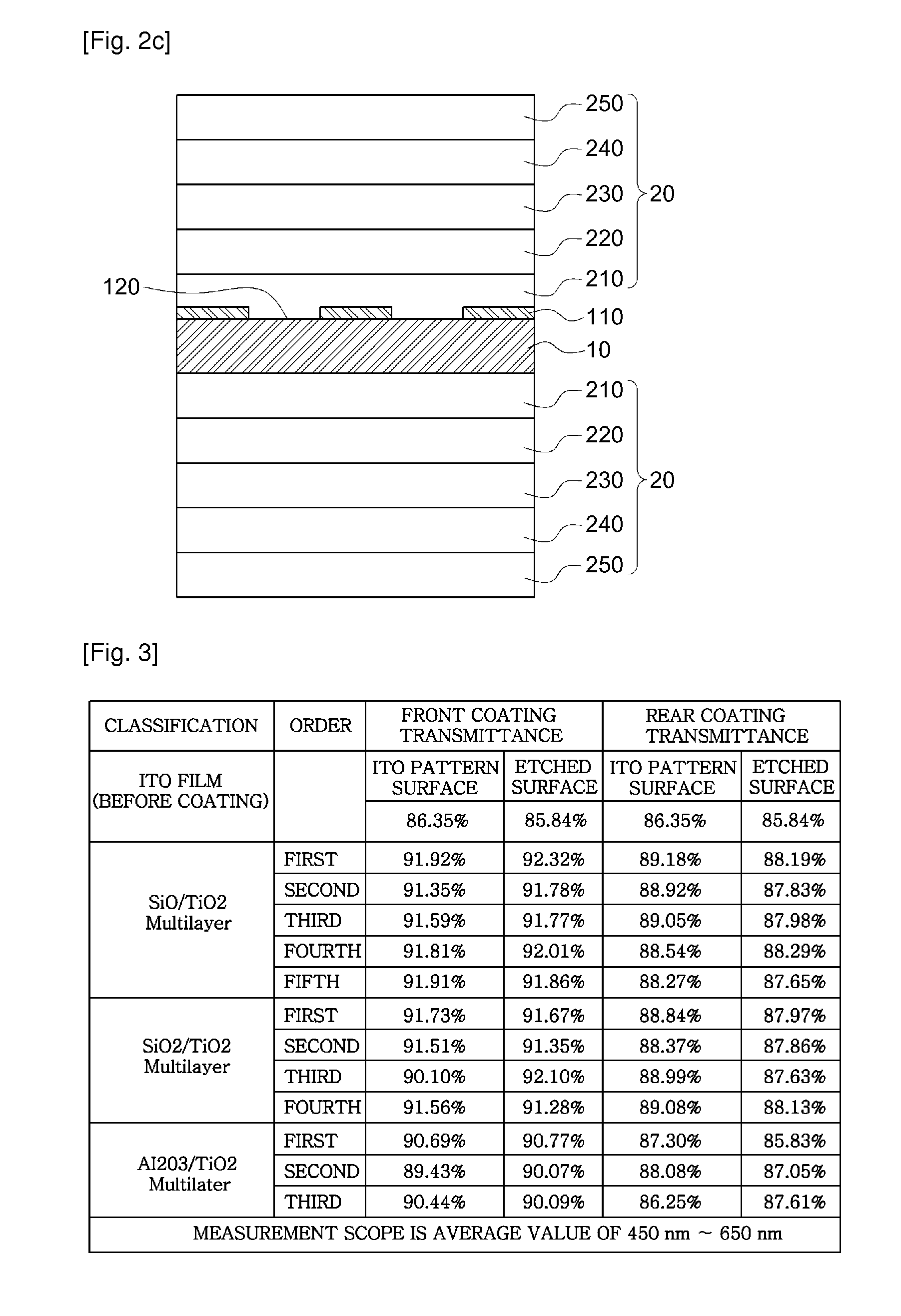
[0060]The third exemplary embodiment of the conductive film with a high transmittance and having a number of anti reflection coated films (20) is a configuration where the number of anti reflection coated films (20) is coated on all the front and rear surfaces to further increase the transmittance and yet to reduce reflectivity, as shown in FIG. 2c.
[0061]In third exemplary embodiment, the number of anti reflection coated films (20) are formed on front and rear surfaces of the conductive film (10) formed with the transparent electrode pattern (110), such that material of film at each layer, the number of layers at each film, and thickness of each film (described later) are same as those of the first and second exemplary embodiments.
experimental examples
[0062]FIG. 3 is a table illustrating an optical transmittance according to each exemplary embodiment of a conductive film with a high transmittance and having a number of anti reflection coated film (20) according to the present invention.
[0063]In the experimental example, the transparent electrode pattern (110) is formed on the conductive film (10) as a test pattern, where the transparent electrode pattern (110) and the etching surface (120) are all provided with a thickness of 3 cm. As illustrated in FIG. 3, it could be noted that a high transmittance (T %) was produced from most of the optical wavelengths of 450 nm˜650 nm under conditions of the following Tables 1 to 6.
[0064]In a case the first layer film (210), which is a base film for the conductive film, is made of silicon monoxide, thickness of each film at each layer of the AR films in the first exemplary embodiment of conductive film with a high transmittance (front coating for the conductive film 10) is as provided in the ...
PUM
 Abstract
Description
Claims
Application Information
 - R&D
- Intellectual Property
- Life Sciences
- Materials
- Tech Scout
- Unparalleled Data Quality
- Higher Quality Content
- 60% Fewer Hallucinations
Browse by: Latest US Patents, China's latest patents, Technical Efficacy Thesaurus, Application Domain, Technology Topic, Popular Technical Reports.
© 2025 PatSnap. All rights reserved.Legal|Privacy policy|Modern Slavery Act Transparency Statement|Sitemap|About US| Contact US: help@patsnap.com


