
Solid-state imaging device, method for driving solid-state imaging device, and electronic apparatus

a solid-state imaging and imaging device technology, applied in the direction of radio frequency controlled devices, instruments, television systems, etc., can solve the problems of reducing the conversion efficiency of charge-to-voltage, not suitable for pixel size reduction, and not suitable for miniaturization, so as to prolong the charge retention time of the charge storage capacitor, improve noise immunity, and reduce the conversion efficiency of the fd part.

Active Publication Date: 2013-03-21
SONY GRP CORP
View PDF3 Cites 7 Cited by
  • Summary
  • Abstract
  • Description
  • Claims
  • Application Information

AI Technical Summary

Benefits of technology

The solution enables high integration with improved noise immunity and charge retention time while maintaining conversion efficiency, allowing for a global shutter function with fewer components and simplified driving circuits, suitable for miniaturization.

Problems solved by technology

However, the large capacitance value of the charge storage capacitor causes an increase in capacitance of the floating diffusion part, which results in a decrease in charge-to-voltage conversion efficiency.
Hence, the related art technique described in Japanese Unexamined Patent Application Publication No. 11-177076 is not suitable for pixel size reduction.
Therefore, the related art technique described in Japanese Unexamined Patent Application Publication No. 11-177076 is not suitable for miniaturization.
Besides, since KTC noise upon reset may not be removed, it is difficult to suppress pixel-specific fixed pattern noise.
This increases the number of components that are to be integrated in one pixel, thereby making high integration difficult.
Moreover, two reset signal lines are necessary at least for pixel reset, which complicates the structures of peripheral driving circuits for driving pixels.

Method used


Image

  • Solid-state imaging device, method for driving solid-state imaging device, and electronic apparatus
  • Solid-state imaging device, method for driving solid-state imaging device, and electronic apparatus
  • Solid-state imaging device, method for driving solid-state imaging device, and electronic apparatus

Examples


embodiment

2. Embodiment

[Circuit Structure]

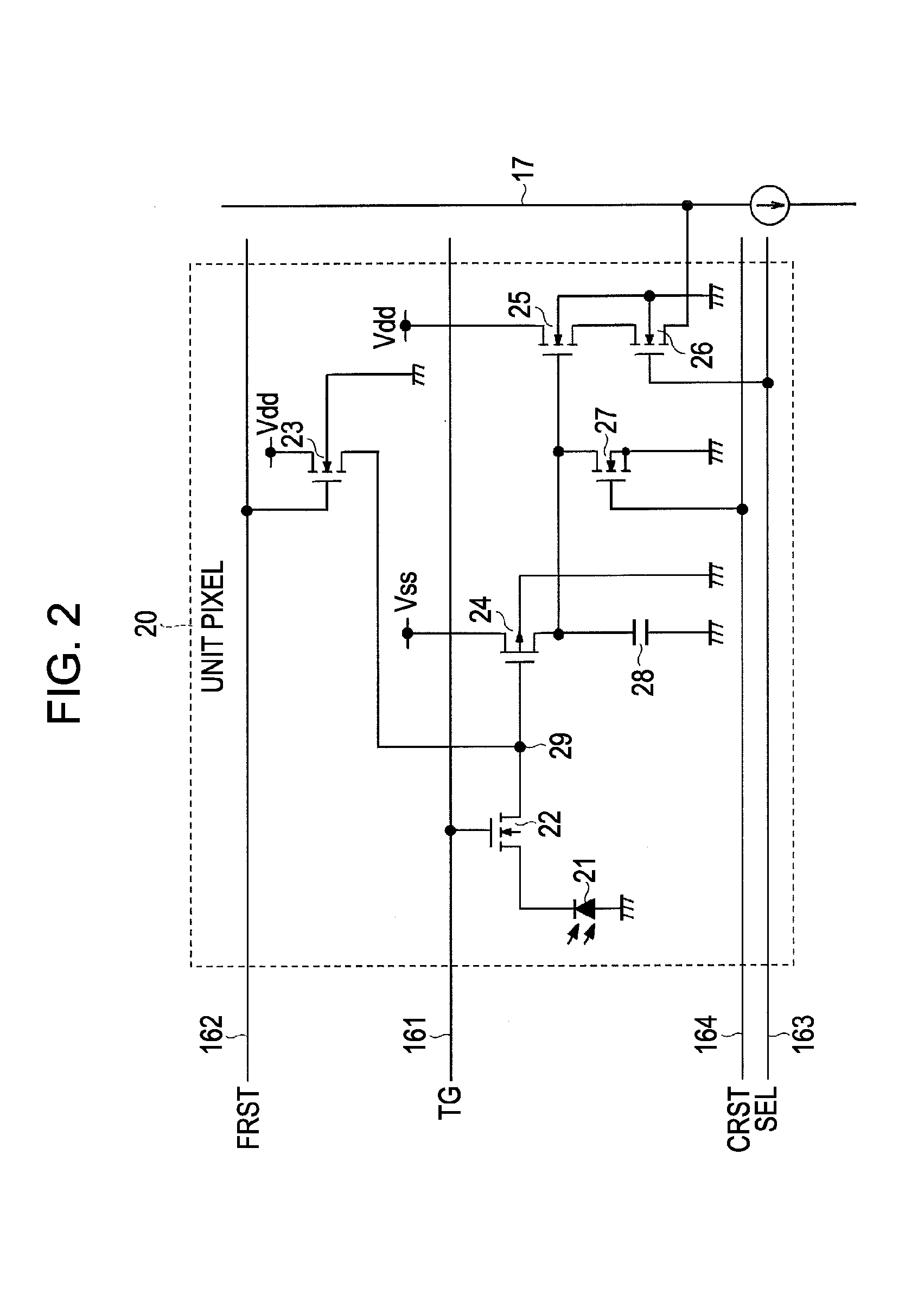
[0045]FIG. 2 is a circuit diagram showing a circuit structure of the unit pixel 20 according to an embodiment. As shown in FIG. 2, the unit pixel 20 according to the embodiment includes, for example, six transistors 22 to 27 and one capacitor 28, in addition to, for example, a photodiode 21 which is a photoelectric conversion part. The capacitor 28 is the charge storage capacitor for achieving the global shutter function.

[0046]For instance, N-channel MOS transistors are used as the transistors 22, 23, and 25 to 27 and a depression type MOS transistor is used as the transistor 24. However, the conductivity type combination of the transistors 22 to 27 exemplified here is merely an example, and the conductivity type combination is not limited to such.

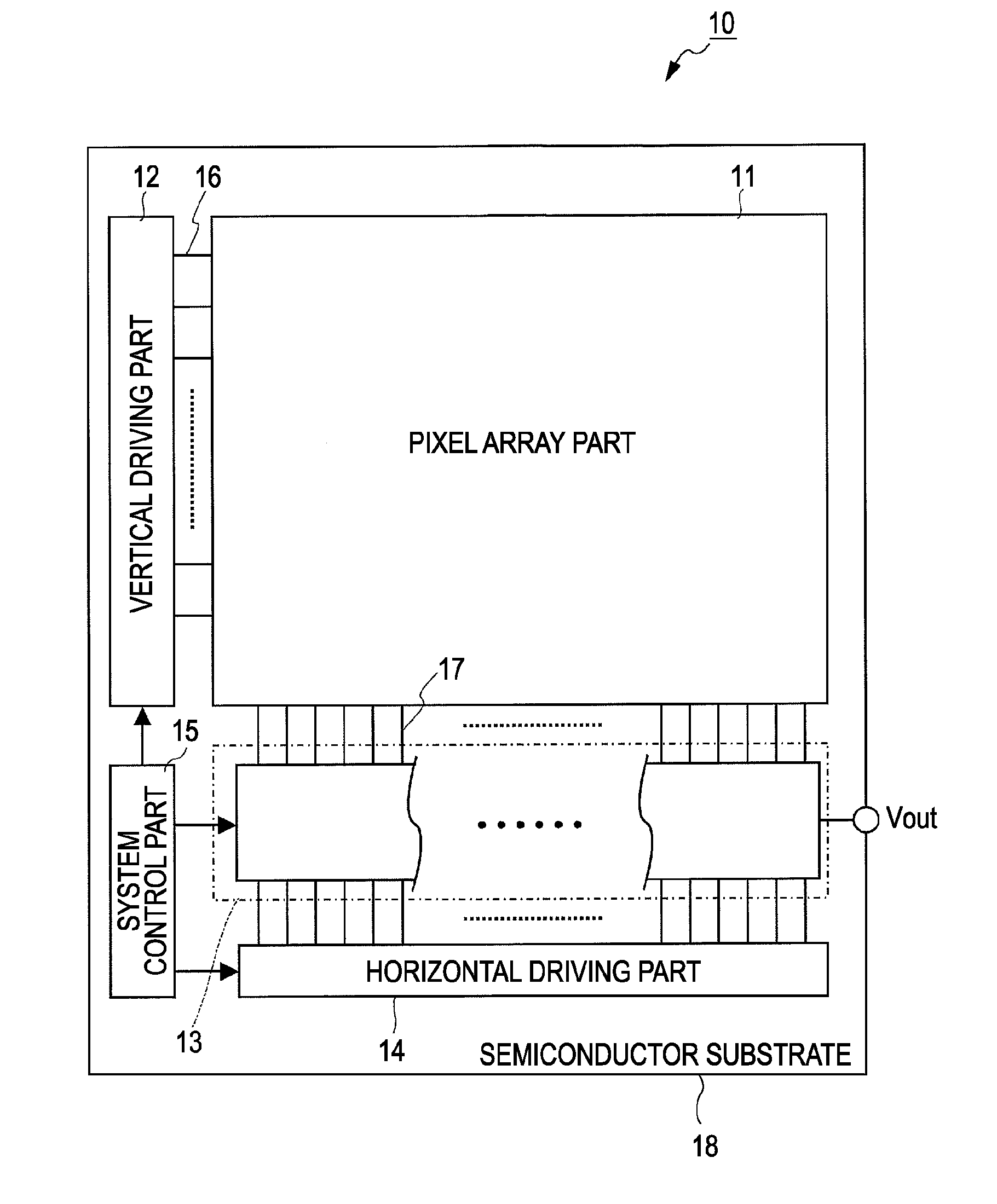
[0047]For this unit pixel 20, for example, four pixel driving lines of a transfer line 161, a first reset line 162, a selection line 163, and a second reset line 164 are wired as the pixel driving line 16 so...


PUM

PropertyMeasurementUnit
chargeaaaaaaaaaa
chargesaaaaaaaaaa
currentaaaaaaaaaa

Abstract

A solid-state imaging device comprising a plurality of unit pixels each comprising (a) a photoelectric conversion element operative to generate a charge in response to incident light, (b) a first storage element in which the charge generated by the photoelectric conversion element is stored and (c) a second storage element in which a charge based on the charge stored in the first storage element is stored, wherein, for each pixel, the second storage element is located at an opposite side of a light receiving surface of the photoelectric conversion element.

Description

RELATED APPLICATION DATA[0001]This application is a continuation of U.S. patent application Ser. No. 12 / 717,515, filed Mar. 4, 2010, the entirety of which is incorporated herein by reference to the extent permitted by law. This application claims the benefit of priority to Japanese Patent Application No. JP 2009-058984 filed in the Japanese Patent Office on Mar. 12, 2009, the entirely of which is incorporated herein by reference to the extent permitted by law.BACKGROUND OF THE INVENTION[0002]1. Field of the Invention[0003]The present invention relates to a solid-state imaging device, a method for driving the solid-state imaging device, and an electronic apparatus. The present invention particularly relates to an X-Y address type solid-state imaging device having a global shutter function, a method for driving the solid-state imaging device, and an electronic apparatus including the solid-state imaging device.[0004]2. Description of the Related Art[0005]There are two main types of so...

Claims


Application Information

Patent Timeline
Patent Type & Authority Applications(United States)
IPC IPC(8): H04N5/335H01L27/148H01L27/146H04N25/00
CPCH01L27/14609H01L27/14621H01L27/14627H01L27/14636H01L27/14641H04N5/353H04N5/37457H01L27/1464H01L27/14643H04N25/778H04N25/532H04N25/53
Inventor WATANABE, KAZUFUMI
Owner SONY GRP CORP
Learn More