
Ips pixel unit, liquid crystal display and image control method

a liquid crystal display and pixel unit technology, applied in the field of ips pixel units and lcds, can solve the problems of low brightness level, reduced aperture ratio (i), size of bright regions, etc., and achieve the effect of low power consumption, high brightness level and reduced resolution

Inactive Publication Date: 2013-03-14
SHENZHEN CHINA STAR OPTOELECTRONICS TECH CO LTD
View PDF2 Cites 2 Cited by
  • Summary
  • Abstract
  • Description
  • Claims
  • Application Information

AI Technical Summary

Benefits of technology

The present invention provides an IPS pixel unit and an LCD comprising the same that can improve the aperture ratio and resolution when switching between 3D and 2D modes. The invention achieves this by dividing the electrodes of one pixel unit into at least two regions, which allows for independent control of brightness levels for each region. As a result, the display will have high brightness levels and low power consumption in the 2D mode, while also increasing the resolution without compromising the aperture ratio.

Problems solved by technology

Consequently, when the IPS display switches from the 3D displaying mode to the 2D displaying mode, the BM photomask that masks a portion of the pixel regions at all times will cause pixel electrodes in the portion of pixel regions to become dark, which results in a decreased aperture ratio (i.e., the size of the bright region), a low brightness level and higher power consumption.

Method used


Image

  • Ips pixel unit, liquid crystal display and image control method
  • Ips pixel unit, liquid crystal display and image control method
  • Ips pixel unit, liquid crystal display and image control method

Examples


Embodiment Construction

[0031]For better understanding of the objectives, technical solutions and advantages of the present disclosure, the present disclosure will be further detailed with reference to embodiments thereof and the attached drawings. It shall be understood that, the embodiments described herein are only intended to illustrate but not to limit the present disclosure.

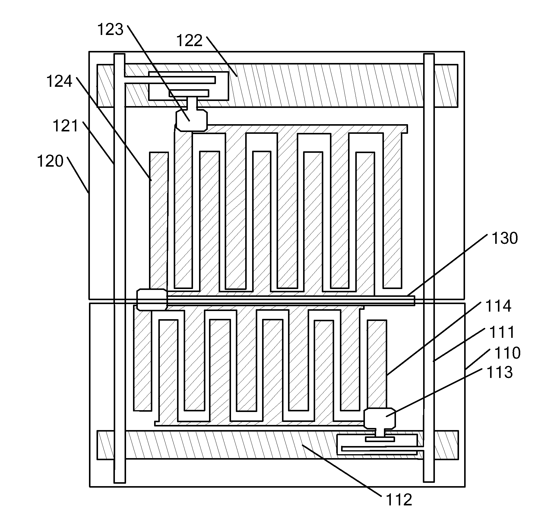
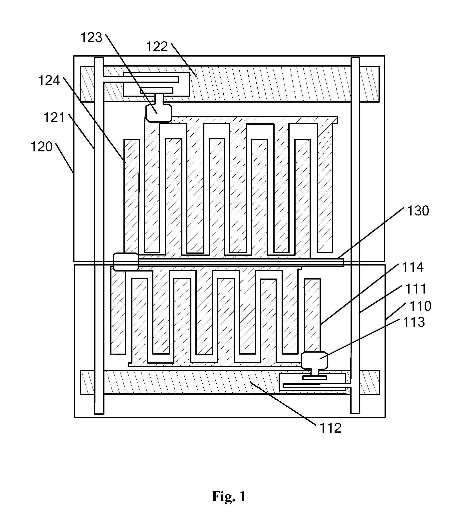
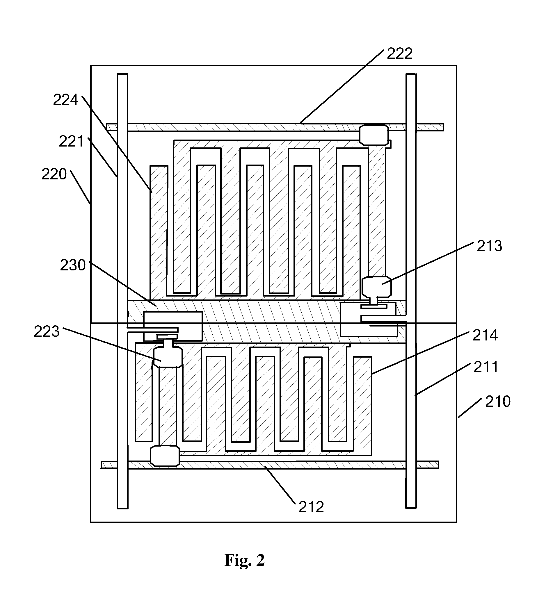
[0032]Referring to FIG. 1, there is shown a schematic structural view of a first embodiment of an in-plane switch (IPS) pixel unit according to the present disclosure. The IPS pixel unit is divided into a first pixel electrode region 110 and a second pixel electrode region 120. The first pixel electrode region 110 comprises first pixel electrodes 114, a first signal line 111, a first voltage switch module 113 and a first control switch 112. The second pixel electrode region 120 comprises second pixel electrodes 124, a second signal line 121, a second voltage switch module 123 and a second control switch 122. A grounding terminal 1...


PUM


Abstract

An in-plane switch (IPS) pixel unit comprises: a plurality of pixel electrodes, signal lines, voltage switch modules and control switches. The pixel electrodes are divided into at least two pixel electrode regions respectively connected to the signal lines via one voltage switch module; the control switches controls connection with the voltage switch modules respectively; and the signal lines supply voltage signals to the pixel electrodes through the control of the control switches over the voltage switch modules. With the IPS pixel unit, when the display switches from a three-dimensional (3D) displaying mode to a two-dimensional (2D) displaying mode, the aperture ratio of the display remains unchanged, and the display will have a high brightness level and low power consumption; and a situation where the number of available pixels in is decreased to cause a lower resolution and more significant black lines is avoided, the resolution of the display is increased.

Description

BACKGROUND[0001]1. Technical Field[0002]The present disclosure relates to the technical field of liquid crystal displays (LCDs), and more particularly, to an in-plane switch (IPS) pixel unit, an LCD comprising the same and an image control method.[0003]2. Description of Related Art[0004]In in-plane switch displays of the prior art, pixels are not divided into different regions. In order to avoid the cross-talk occurring at large viewing angles when a polarizing 3D IPS display is used, a wide black matrix (BM) photomask must be made in the pixels of the IPS display to mask pixel electrodes in a portion of pixel regions so as to block the light traveling to pixel electrodes located at large viewing angles or to turn off pixel electrodes of a whole region. In this way, a 3D effect can be achieved.[0005]However, when the practice of making a wide BM photomask to block light traveling to pixel electrodes located at large viewing angles is adopted, the BM photomask of the prior art masks ...

Claims


Application Information

Patent Timeline
IPC IPC(8): G09G3/36G09G5/00G09G3/20
CPCG09G3/003G09G2310/061G09G2300/0434G09G3/3648
Inventor HOU, HUNG-LUNGHE, CHENGMING
Owner SHENZHEN CHINA STAR OPTOELECTRONICS TECH CO LTD
Learn More