
Power converter

a power converter and converter technology, applied in the direction of electric variable regulation, process and machine control, instruments, etc., can solve the problem of limiting the maximum output power of the power converter, and achieve the effects of reducing the temperature of the fet, increasing the heat generation of the freewheel diodes, and reducing the heat generation of the fets

Active Publication Date: 2013-01-03
MITSUBISHI ELECTRIC CORP
View PDF7 Cites 27 Cited by
  • Summary
  • Abstract
  • Description
  • Claims
  • Application Information

AI Technical Summary

Benefits of technology

The patent text describes a method to increase the power conversion of a power converter by reducing heat generation in the FETs (semiconductor switches) and increasing heat generation in the free wheel diodes. This is achieved by skipping ON signals of the PWM gate signals when the current flow is negative. The technical effect is an elevated maximum output power of the power converter.

Problems solved by technology

Hence, there arises a problem that the temperatures of the FETs limit maximum output power of the power converter.

Method used


Image

  • Power converter
  • Power converter
  • Power converter

Examples


first embodiment

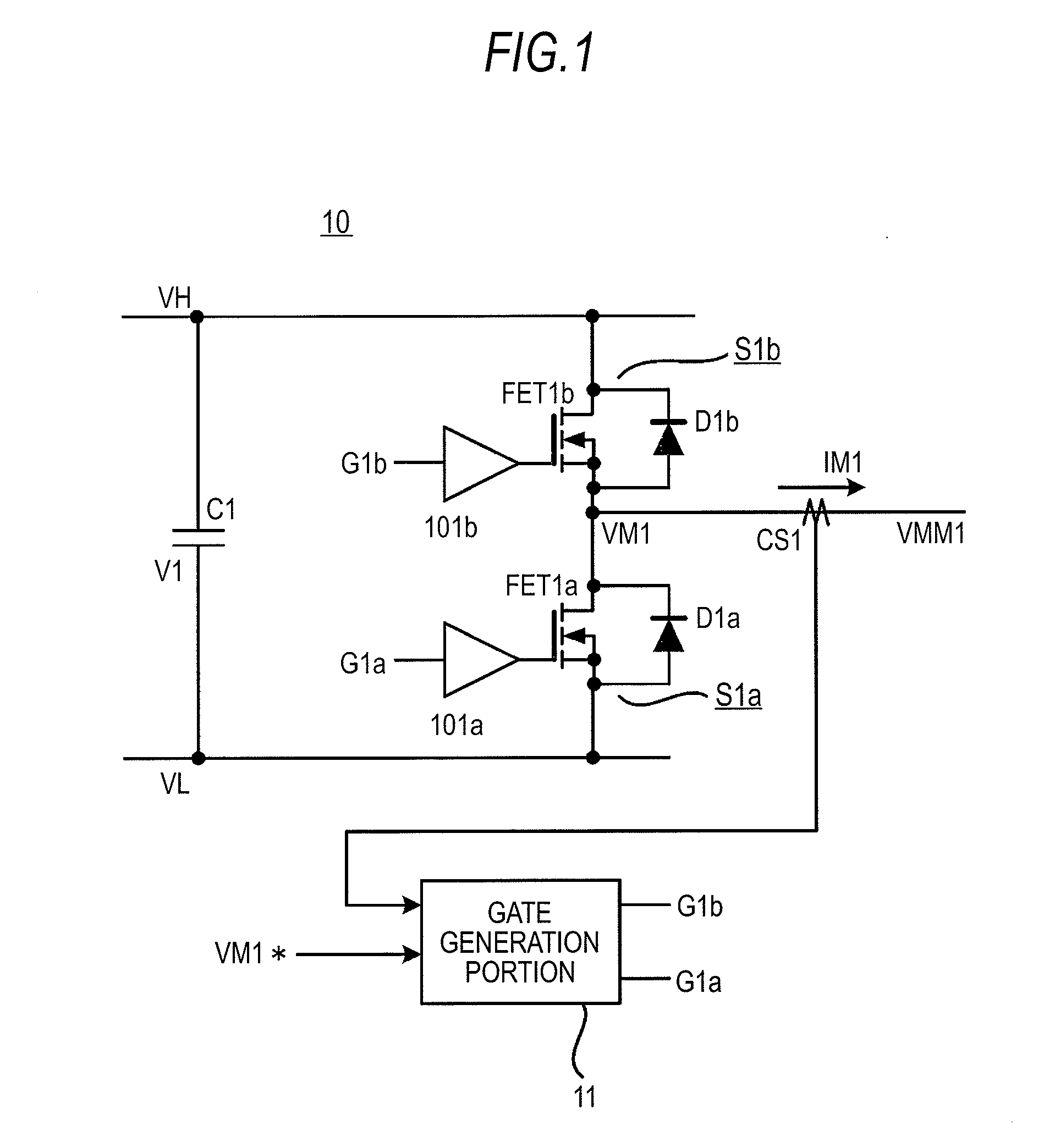
[0027]FIG. 1 is an electric circuit diagram showing a configuration of a main circuit and a control portion of a power converter according to a first embodiment of the invention.

[0028]A power converter 10 of the first embodiment is a voltage-sourced power converter furnished with a capability of converting a DC voltage V1 between a voltage terminal VH and a voltage terminal VL to a square-wave voltage by complementary switching actions of one set of semiconductor switches S1a and S1b and outputting the resulting voltage to a voltage terminal VM1.

[0029]Referring to FIG. 1, the power converter 10 includes a smoothing capacitor C1 that smoothes the DC voltage V1, one set of the semiconductor switches S1a and S1b, a current sensor CS1 as a portion detecting a current flowing through the semiconductor switches S1a and S1b, and a gate generation portion 11.

[0030]The semiconductor switches S1a and S1b in one set are formed of FET1a and FET1b, which are FETs using a wide band-gap semiconduc...

second embodiment

[0090]A power converter according to a second embodiment of the invention will now be described. FIG. 11 is an electric circuit diagram showing a configuration of a main circuit and a control portion of the power converter of the second embodiment.

[0091]A power converter 20 of the second embodiment is a voltage-sourced power converter furnished with a capability of converting a DC voltage V1 between a voltage terminal VH and a voltage terminal VL to a voltage having three types of potential by switching actions of two sets of semiconductor switches S2a and S2b and semiconductor switches S3a and S3b and outputting the resulting voltage to a voltage terminal VM1. The power converter 10 of the first embodiment above obtains a voltage (square-wave voltage) having two types of potential and outputs the resulting voltage to the voltage terminal VM1. In contrast, the power converter 20 of the second embodiment is a three-level voltage-sourced power converter that obtains a voltage having t...


PUM


Abstract

A power converter has one set of two semiconductor switches performing switching actions, each of which is formed of an FET and a free wheel diode connected in anti-parallel to the FET, and a smoothing capacitor, and convers power by complementary switching actions of the FETs in the semiconductor switches. The power converter is provided with a current sensor that detects a direction of a current flowing through the semiconductor switches and a gate generation portion that skips ON signals of PWM gate signals of the semiconductor switches when the direction of the current flowing through the semiconductor switches is negative.

Description

BACKGROUND OF THE INVENTION[0001]1. Field of the Invention[0002]The present invention relates to a power converter using a field effect transistor and a diode.[0003]2. Description of the Related Art[0004]As a power converter using a wide band-gap semiconductor device in the related art, there is a voltage-sourced power converter. This power converter has two semiconductor switches each of which is formed of an FET (Field Effect Transistor) using a wide band-gap semiconductor and a free wheel diode using a wide band-gap semiconductor and connected inversely in parallel (connected in anti-parallel) to the FET. These two semiconductor switches are connected to a capacitor functioning as a voltage source. The power converter converts power by complementary switching actions of the FETs in the two semiconductor switches.[0005]An FET and a diode both using a wide band-gap semiconductor are operable at high temperatures and have a small switching loss relative to an IGBT and a diode both u...

Claims


Application Information

Patent Timeline
Patent Type & Authority Applications(United States)
IPC IPC(8): G05F3/02
CPCH02M2001/327H02M7/5387H02M1/088H02M1/0054H02M1/0009H01L2224/32225H01L2924/13055H02M1/327H02M7/4837Y02B70/10H01L2924/00H02M3/3376H02M3/156
Inventor IKEDA, MATAHIKOKOBAYASHI, MASARUMORITAKE, NAOKIMITSUI, TAKAOMAEKAWA, HIROTOSHIISHIBASHI, SATOSHIIDENOUE, SHINSUKE
Owner MITSUBISHI ELECTRIC CORP
Learn More