
Thin film photovoltaic cell, a method for manufacturing, and use

Inactive Publication Date: 2013-01-03
BENEQ OY
View PDF5 Cites 13 Cited by
  • Summary
  • Abstract
  • Description
  • Claims
  • Application Information

AI Technical Summary

Benefits of technology

The present invention relates to a new photovoltaic cell device that uses a material called Zn(O,S) to enhance the efficiency of a solar cell. Zn(O,S) has physical and chemical properties that make it compatible with CdTe, allowing for a good pn-junction between these materials. Additionally, the bandgap of Zn(O,S) is wider than that of CdS, which improves the conversion of solar energy into electricity. The invention also reduces the amount of toxic cadmium in the device. The invention uses a thin film technology called atomic layer deposition (ALD) to deposit a layer of n-type semiconductor window layer material. The ALD process ensures accurate and controlled deposition of the coating layer, resulting in good conformity and a uniform thickness of the window layer covering the underlying device layers.

Problems solved by technology

This means that a production plant configured to produce cells of one type is not straightforwardly transformable for manufacturing of some other cell type.
This typically compels the thin film photovoltaic cell manufacturers to select one of those technologies only.
There is, however, one well known problem associated with CdS.
This is a significant problem e.g. in solar cells converting the solar radiation into electrical energy.
However, another problem arising along with the CdS layer thinning is the possible pinhole formation creating localized junctions between CdTe and the upper transparent conductive oxide TCO current collecting layer usually present above CdS.
These kinds of points of direct contact between CdTe and TCO would deteriorate drastically the device performance.

Method used


Image

  • Thin film photovoltaic cell, a method for manufacturing, and use
  • Thin film photovoltaic cell, a method for manufacturing, and use
  • Thin film photovoltaic cell, a method for manufacturing, and use

Examples


Embodiment Construction

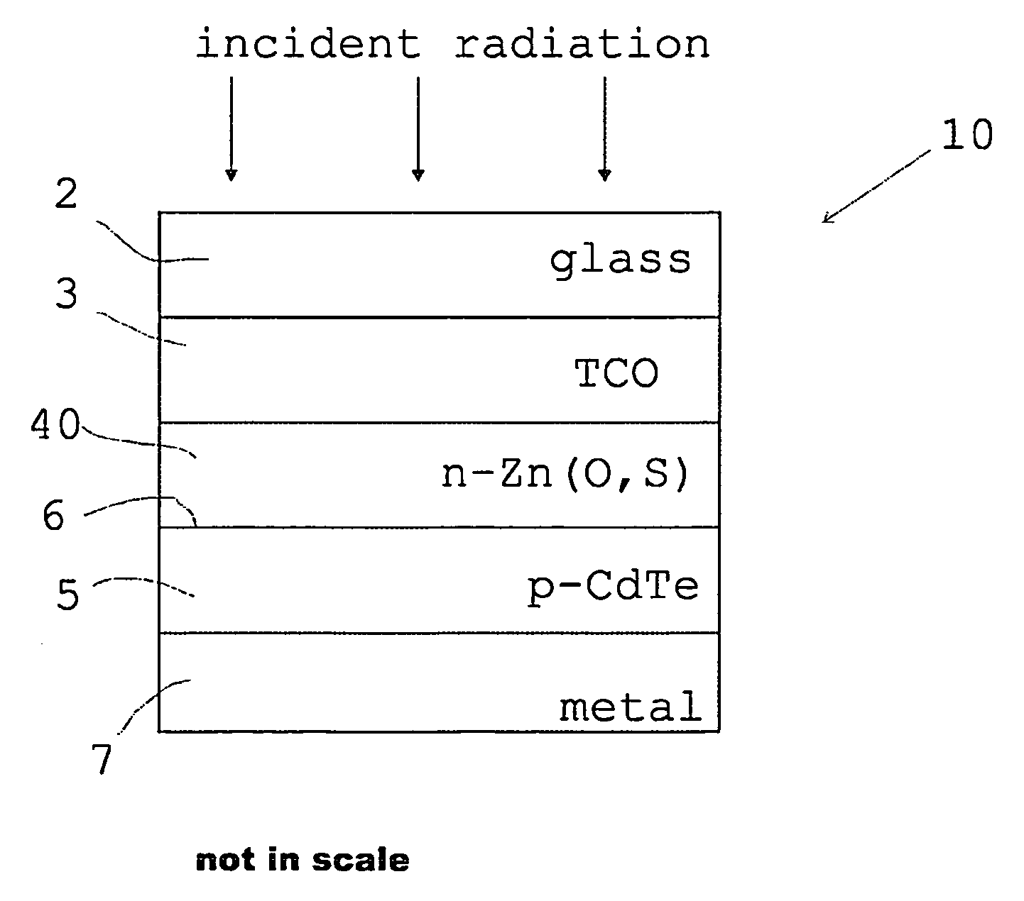
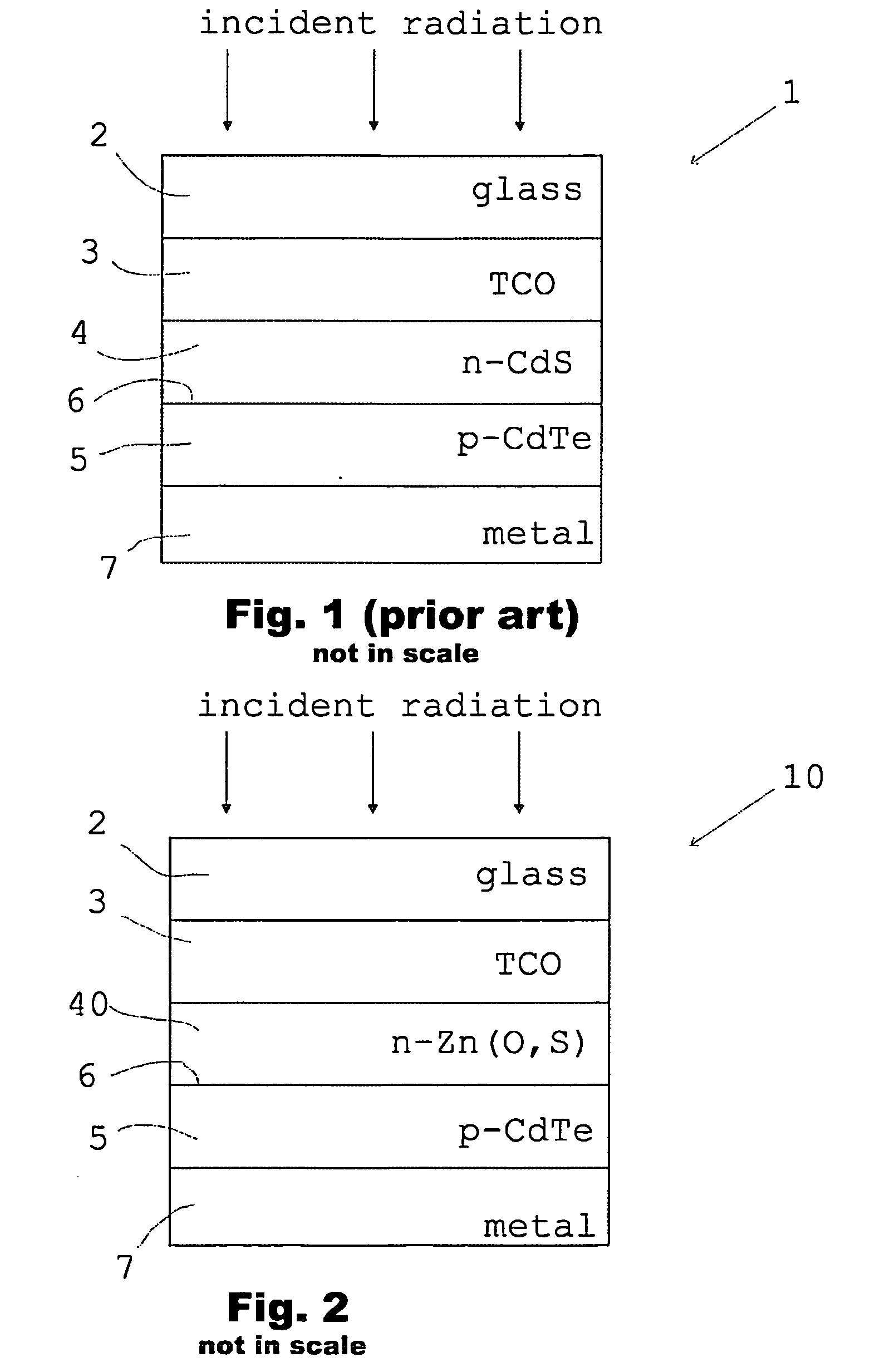
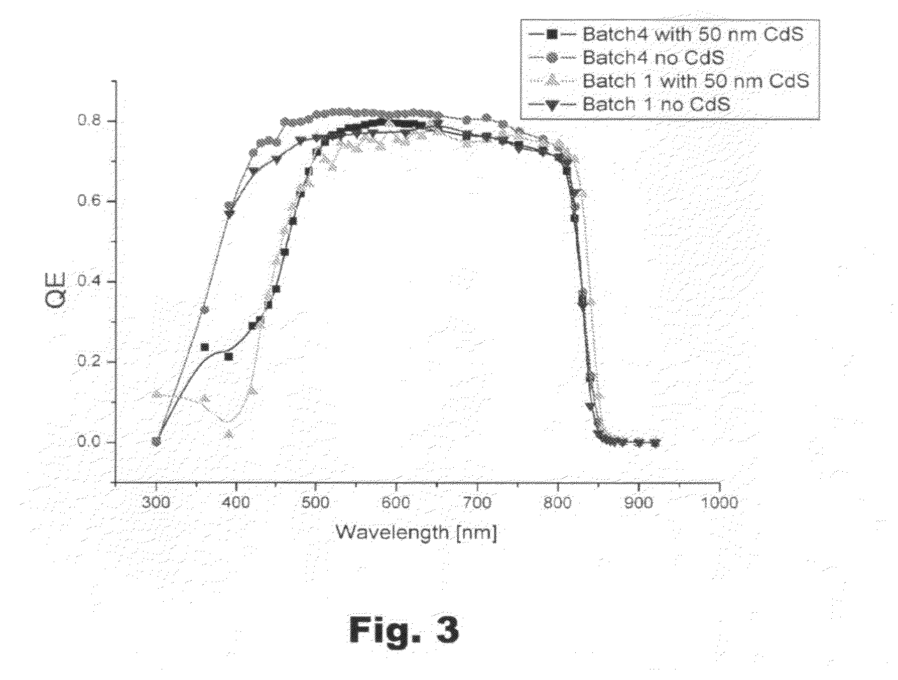
[0028]The present invention is described in more detail in the following by means of the accompanying figures where

[0029]FIG. 1 shows a typical prior art CdTe photovoltaic cell structure,

[0030]FIG. 2 shows schematically one CdTe photovoltaic cell structure according to the present invention,

[0031]FIG. 3 shows a comparison of the relative quantum efficiencies between a prior art device and a CdTe photovoltaic cell according to the present invention, and

[0032]FIG. 4 shows as a flow chart one possible manufacturing method for producing a window layer of a CdTe photovoltaic cell according to the present invention.

[0033]The prior art CdTe / CdS photovoltaic cell 1 of FIG. 1 is formed on a glass substrate 2 which in the figure is the uppermost layer of the device. A transparent conductive oxide TCO layer 3, comprising e.g. fluorine doped tin oxide FTO deposited on the substrate, forms a transparent current collecting layer. Below the TCO layer is an n-doped CdS window layer 4. Adjacent to t...


PUM


Abstract

A thin film photovoltaic cell (10) comprises an n-type semiconductor window layer (40), a p-type semiconductor absorption layer (5) and a pn-junction (6) at the interface between these two layers, wherein the p-type semiconductor absorption layer is formed of cadmium telluride CdTe. According to the present invention, the n-type semiconductor window layer (40) comprises zinc oxide / sulfide Zn (O,S).

Description

FIELD OF THE INVENTION[0001]The present invention relates, in general, to photovoltaic cells. It is directed at the semiconductor layer structure forming the key operational portion of a photovoltaic cell. In more detail, the present invention is focused on Cadmium Telluride (CdTe) based photovoltaic cells, particularly on the n-type semiconductor layers, i.e. the so called window layers of such cells.BACKGROUND OF THE INVENTION[0002]Photovoltaic cells are used in a great variety of applications to convert electromagnetic radiation to electrical energy. One particular field within the photovoltaic cell industry and business is the field of solar cells utilizing sunlight as the primary energy source.[0003]By photovoltaic cell is meant here generally a semiconductor-based component converting incident electro-magnetic radiation to electrical energy through a photovoltaic effect. The simplified basic structure of a photovoltaic cell of the type discussed here typically comprises a wind...

Claims


Application Information

Patent Timeline
IPC IPC(8): H01L31/0296H01L31/18H01L31/0272H01L31/072
CPCH01L31/0296H01L31/02963Y02E10/543H01L31/1828H01L31/1836H01L31/072Y02P70/50
Inventor SKARP, JARMO
Owner BENEQ OY
Learn More