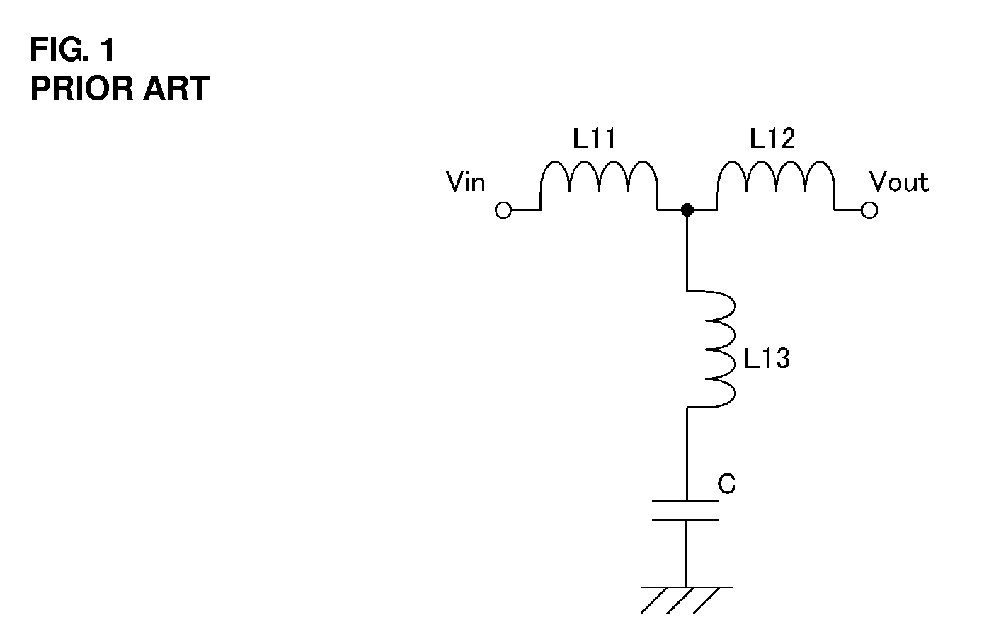
Filter circuit

a filter circuit and circuit technology, applied in the field of filter circuits, can solve the problems of affecting the filter characteristics, the inductance risk of the inductors lb>11/b>, and the inductance risk of the inductors, so as to reduce the magnetic flux density, prevent the inductance change due to the coupling between the inductors, and reduce the risk of inductan

Active Publication Date: 2012-11-01
MURATA MFG CO LTD
View PDF2 Cites 2 Cited by
  • Summary
  • Abstract
  • Description
  • Claims
  • Application Information

AI Technical Summary

Benefits of technology

[0016]In this configuration, as a result of the directions of the magnetic fluxes of the first, second, and third inductors being the same, the magnetic flux density is reduced by the magnetic fluxes canceling each other out and the risk of inductances of the first, second, and third inductors being affected by the magnetic fluxes is minimized. Furthermore, by making the directions of the magnetic fluxes be the same, changing of the inductances due to coupling between the inductors is prevented.
[0017]According to various preferred embodiments of the present invention, even when a misalignment occurs, the effect on the filter characteristics of the filter circuit is prevented or minimized since the inductances of the first inductor, the second inductor, and the third inductor each change by the same or substantially the same proportion.

Problems solved by technology

However, when a multilayer body is constructed by stacking dielectric layers on top of one another, since misalignment sometimes occurs between the dielectric layers, there is a risk of the inductances of the inductors L11, L12 and L13 described in Japanese Unexamined Patent Application Publication No. 2007-129565 being changed.
In addition, there is a risk that the mutual inductance will be changed by a deviation in the distance between the inductors L11, L12 and L13 and that this will affect the filter characteristics.

Method used


Image

  • Filter circuit
  • Filter circuit
  • Filter circuit

Examples


Embodiment Construction

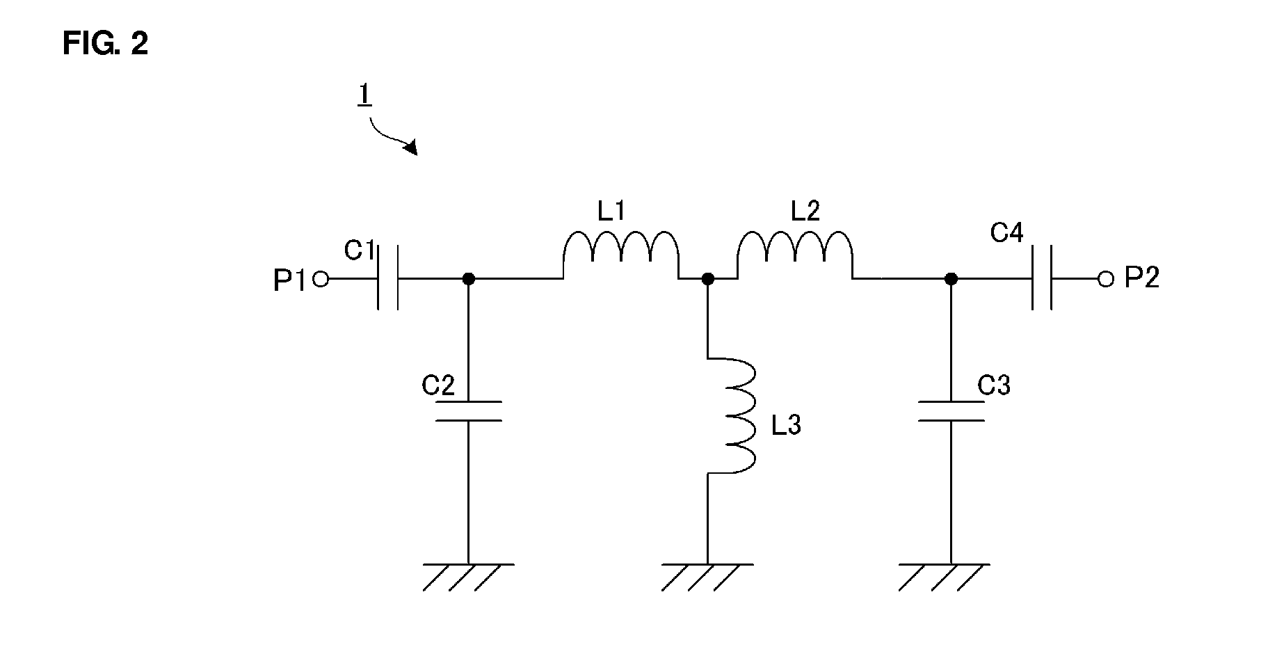
[0024]Hereafter, preferred embodiments of a filter circuit according to the present invention will be described which reference to the drawings. In the preferred embodiments to be described below, the filter circuit according to a preferred embodiment of the present invention will be described as a bandpass filter (hereafter, BPF) having band pass characteristics.

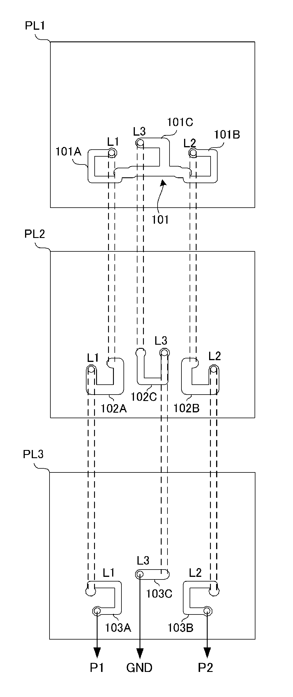
[0025]FIG. 2 illustrates a schematic equivalent circuit of a BPF according to a preferred embodiment of the present invention. A BPF 1 according to the present preferred embodiment preferably includes a multilayer body including a plurality of dielectric layers stacked on top of one another, and electrode patterns (conductive patterns) provided on the dielectric layers. Input / output terminals, a ground potential, inductors, capacitors, signal lines and other suitable circuit elements, for example, which will be described below, are preferably defined by the electrode patterns.

[0026]The BPF 1 preferably includes an input ter...


PUM


Abstract

A bandpass filter includes a multilayer body, which includes a plurality of dielectric layers stacked on top of one another, a first inductor and a second inductor connected in series with each other, and a third inductor connected to a connection point between the first and second inductors, and a ground potential. The first inductor is defined by substantially open-loop-shaped first electrode patterns provided on the dielectric layers being superposed with one another in the stacking direction of the multilayer body. The second inductor and the third inductor are defined by second electrode patterns and third electrode patterns provided on the dielectric layers being superposed with one another in the stacking direction.

Description

BACKGROUND OF THE INVENTION[0001]1. Field of the Invention[0002]The present invention relates to filter circuits that include inductors connected in a T-shaped pattern.[0003]2. Description of the Related Art[0004]In the related art, a variety of filter circuits that include inductors have been designed. FIG. 1 is a circuit diagram illustrating a filter circuit described in Japanese Unexamined Patent Application Publication No. 2007-129565. The filter circuit illustrated in FIG. 1 is a T-circuit low pass filter in which two inductors L11 and L12 are connected in series with each other and in which a point between these two inductors is connected to the ground via an inductor L13 and a capacitor C. The filter circuit illustrated in FIG. 1 includes inner layer electrode patterns of a multilayer body formed by stacking a plurality of dielectric layers on top of one another.[0005]The filter circuit described in Japanese Unexamined Patent Application Publication No. 2007-129565 is configu...

Claims


Application Information

Patent Timeline
Patent Type & Authority Applications(United States)
IPC IPC(8): H03H7/01
CPCH01P1/20345H03H2001/0085H03H7/0115
Inventor YAMAGUCHI, KIYOSHI
Owner MURATA MFG CO LTD
Why Eureka
Try Eureka