Interconnection Interface Using Twist Pins for Testing and Docking

a twist pin and interconnection interface technology, applied in the direction of coupling device details, coupling device connection, instruments, etc., can solve the problems of significant risk of a new chip being defective, chip level testing is difficult, and the twist pin has not been used in interconnection interface testing of high-performance integrated circuits. , to achieve the effect of eliminating differential force distribution, minimizing or eliminating anomalous signal effects, and eliminating differential force distribution

Inactive Publication Date: 2012-08-16
MEDALLION TECH
View PDF5 Cites 17 Cited by
  • Summary
  • Abstract
  • Description
  • Claims
  • Application Information

AI Technical Summary

Benefits of technology

[0020]The present invention uses twist pins in an interconnect interface or test socket to conduct input signals to and output signals from contact pads of an integrated circuit or chip. Twist pins create a substantially uniform-length signal conduction path, thereby minimizing or eliminating anomalous signal effects created by unequal-length probes or conductors. The twist pins establish substantially uniform contact force with each of relatively different height contact pads on a chip, thereby eliminating differential force distributions that may crack or fracture the chip. The physical size of the twist pin is smaller than known spring probes, thereby permitting closer spacing of the twist pins to contact more or all of the closely-spaced contact pads. The twist pins are maintained in alignment for efficient, rapid and cost-effective registration with the contact pads, to assure mass testing productivity and to assure effective permanent docking. The twist pins effectively interact with contact pads having variations of relative heights and with other types of electrical contacts such as solder balls. In general, the use of twist pins as interconnect interfaces offers significant improvements while eliminating or minimizing the limitations of existing and known interconnect interfaces.
[0022]The twist pins are retained in vias in a support plate or other support structure. Bulges of the twist pins physically contact a sidewall of the vias and create frictional resistance to longitudinal movement of the twist pins within the vias. The UUC and the support plate undergo relative movement to physically contact the ends of the twist pins with the contact pads or other contact areas of the UUC. The twist pins slide within the vias to different degrees to accommodate the differences in relative height of the contact pads. The frictional resistance of the bulge with the sidewall of each via remains approximately constant regardless of the degree of movement of the twist pin in the via. The amount of force of the twist pin against the contact pad is related only to the degree of compression of the bulge against the sidewall of the via. Twist pins having similar bulge characteristics located in vias having similar diameters exert substantially similar forces on each of the contact pads of the UUC, regardless of differences in height of the contact pads and regardless of the difference in movement of each twist pin, unlike the increasing force from a spring probe on a contact pad resulting from the variable compression of the spring probe relative to the height of the contact pad. The uniform force distribution over the UUC, which results from the constant forces exerted by the twist pins on the contact pads, minimizes the risks of cracking or fracturing the chip.
[0023]Since the bulges of the twist pins are located at a constant distance from the contacting ends of the twist pins, and because the signals conducted to or from the twist pins enter or leave the twist pins at the points where the bulges contact the sidewalls of the vias, the twist pins create a substantially consistent signal conduction path to all of the contact pads. The constant length between the points where the bulges contact the sidewalls of the vias has the effect of making the electromagnetic field created by each twist pin more uniform and consistent, which has the practical effect of minimizing variations in cross-talk between signals, minimizing undesired phase relationships and minimizing other anomalous signal effects. The bulges in contact with the sidewalls of the vias create a substantial surface area for transferring the signals, thereby enhancing the quality of the individual signals conducted, since high-frequency signals are conducted more on the surfaces of conductors rather than within the interior of the conductors. In general, the consistent signal conduction path created by the twist pins in vias normalizes or minimizes the anomalous signal-influencing factors and establishes a more uniform quality and relationship of the signals conducted to and from the UUC.
[0024]Twist pins located in the vias of a support plate are also used to create permanent electrical connections with UUCs. The resulting electrical connections are more reliable than lead-free solder connections which are now required in electronic circuit manufacturing. Use of the twist pins in the vias avoids entirely the problems of whisker effects which are created by lead-free solder connections.

Problems solved by technology

Although twist pins have been successfully used as z-axis interconnectors, it is believed that twist pins have not been used in interconnection interfaces for testing high performance integrated circuits, such as microprocessors or memory chips, or for docking electronic components by direct connection to contact pads or surfaces.
Because of the complexity of the integrated circuit manufacturing process and the microscopic size of a large number of electronic components which must be integrated into the single chip in a properly functional and interrelated manner, there is a significant risk that a new chip is defective because of discrepancies which occurred during the manufacturing process.
Chip level testing is difficult because of the high density of closely-spaced small contact pads on the chip.
The close spacing or “pitch” of the contact pads has made it difficult or impossible to establish electrical contact with each of the large number of closely pitched contact pads on a rapidly-occurring, cost-efficient and easily-replicated basis.
Electrical test probes cannot quickly and reliably contact to the contact pads, because such probes usually consume more space than the pitch between the densely positioned contact pads.
Even if space is available, significant operator attention is required to properly position the probes.
Of course, using less than a complete functional tests to evaluate a chip increases the risk that the chip will be determined at a later time to be defective in some regard, thereby increasing manufacturing costs due to packaging a partially defective chip and assembling an electronic product using a package with the partially defective chip.
Making good electrical contact of the probes with the contact pads is further complicated because the chip manufacturing process typically results in contact surfaces on the contact pads which are not located in the same plane.
Since the layers and the components do not necessarily build up evenly and uniformly, it becomes impossible to assure that all of the contact pads on the chip are built up to the same height.
Insufficient contact results in an unreliable electrical path for communicating signals.
An unreliable electrical path may falsely indicate that a chip is functioning incorrectly, when in reality the discrepancy is from the electrical contact with the contact pad and not from the functionality of the chip itself.
Usually a contact force of less than 9 grams per contact will not assure an effective signal path.
Despite the advantages of spring probe test sockets, they present certain limitations.
One limitation involves the physical size of the spring probe itself.
Consequently in most modern chips, it becomes impossible to position the spring probes close enough to each other to achieve registration with the contact pads on the chip while still retaining the spring probes in the desired position in the support plate.
Consequently, the use of spring probes during testing of modern chips is usually limited to partial functionality tests, since electrical contact with all of the contact pads is not possible.
Another limitation of spring probe test sockets is that each individual spring probe applies a different force to the contact pads according to the degree of compression of each spring probe.
Variations in contact force have the potential to create sufficient force differentials over the surface of the chip which could cause the chip to fracture or crack before or after the chip is encapsulated in the package.
A fracture or crack in the chip could also break the bond of a lead to the contact pad.
Another significant limitation on spring probe test sockets is that spring probes degrade the quality of input test signals supplied to the chip and the quality of the output response signals supplied from the chip, particularly at the very high frequencies at which many modern integrated circuits operate.
The electromagnetic radiation of the electrical field from one spring probe influences the signals conducted by adjoining spring probes, in a manner sometimes referred to as “cross-talk.” Variable field effects from one chip to the next makes it difficult or impossible to eliminate the effects of cross-talk on the output response signals.

Method used


Image

  • Interconnection Interface Using Twist Pins for Testing and Docking
  • Interconnection Interface Using Twist Pins for Testing and Docking
  • Interconnection Interface Using Twist Pins for Testing and Docking

Examples


Embodiment Construction

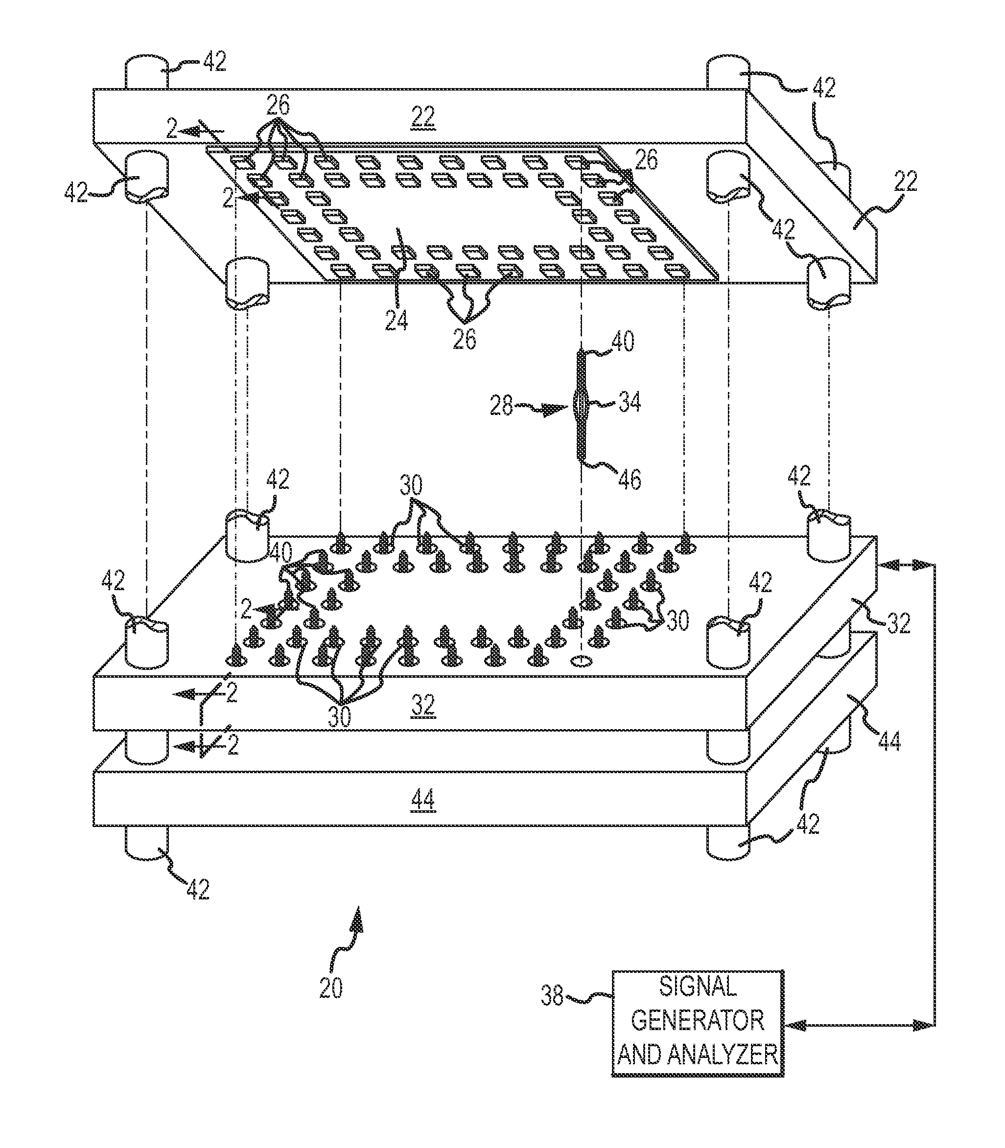
[0036]The present invention may be advantageously incorporated in an interconnect interface having the generalized characteristics illustrated in FIG. 1. The interconnect interface is exemplified by a test socket 20 which includes a retainer plate 22 that holds and positions a unit under connection (UUC) 24. The UUC 24 may be a semiconductor or integrated circuit chip (illustrated), a package or device, a printed circuit board, electronic components or other electrical or electronic products (none shown). Each UUC 24 will have contact pads 26, or other contact surfaces or terminals, located on it by which to receive electrical power, electrical reference potential and input signals to the UUC and from which to deliver output signals from the UUC in response to the input signals.

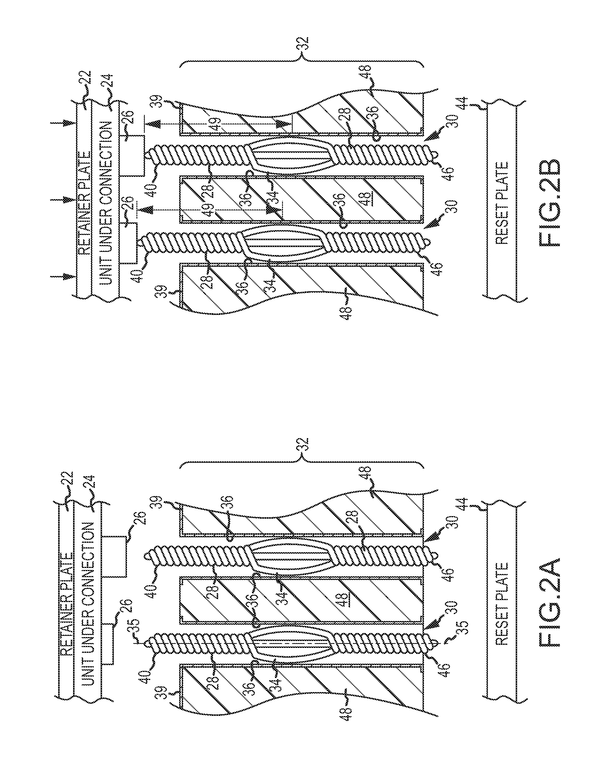
[0037]Twist pins 28 are an important part of the interconnect interface exemplified by the test socket 20. The twist pins 28 conduct the input signals to the contact pads 26 of the UUC 24 and receive the outp...


PUM


Abstract

A twist pin is used as an interconnect interface to conduct signals to and from an electronic component. The twist pin includes a bulge which establishes compressive contact force with a sidewall of a via in which the twist pin resides, and the resulting force resists movement of the end of the twist pin away from the electronic component to assure good signal conductivity. The arrangement may be used as a test socket for testing integrated circuit components or permanently docking electronic components.

Description

[0001]This invention relates to interconnecting electronic components, both on a temporary basis for purposes of testing and on a permanent basis for purposes of creating a product. More particularly, the present invention relates to a new and improved interconnection interface which utilizes twist pins to achieve improved signal conductivity to high-performance electronic components, such as microprocessors, memories and other integrated circuits, on a more reliable, rapidly-accomplished and cost-efficient basis.BACKGROUND OF THE INVENTION[0002]A twist pin is an elongated electrical conductor formed from multiple helically coiled strands of wire. At least one longitudinal segment of the coiled strands is untwisted in an anti-helical direction to expand the strands into a resilient bulge. The bulge has a larger diameter than the diameter of the regularly stranded wires of the adjacent portions of the twist pin on the opposite ends of the bulge. The strands of wire are preferably for...

Claims


Application Information

Patent Timeline
Patent Type & Authority Applications(United States)
IPC IPC(8): H01R12/00
CPCH01R13/2421G01R1/07314G01R1/06716H01R2201/20
Inventor GARCIA, STEVEN E.KOCHER, DOUGLAS R.
Owner MEDALLION TECH
Why Eureka
Try Eureka