Nitrogen-containing aromatic heterocyclic derivative and organic electroluminescence device using the same

Active Publication Date: 2012-07-19
IDEMITSU KOSAN CO LTD
View PDF12 Cites 17 Cited by
  • Summary
  • Abstract
  • Description
  • Claims
  • Application Information

AI Technical Summary

Benefits of technology

[0015]An object of the invention is to provide a novel compound which can be used for an organic EL device. Another object of the invention is to provide an organic EL device which has high luminous efficiency and a long life time, and which can be driven at a low voltage.
[0059]According to the invention, a novel compound which can be used for an organic EL device can be provided. When the compound of the invention is used for a host-transporting material and the like, an organic EL device having high luminous efficiency, low-voltage driving, and a long life time can be achieved.

Problems solved by technology

In addition, in the invention of Patent Document 2, a biscarbazole derivative is used as a phosphorescent emitting host material, and there is concern that luminous efficiency will significantly be deteriorated.

Method used


Image

  • Nitrogen-containing aromatic heterocyclic derivative and organic electroluminescence device using the same
  • Nitrogen-containing aromatic heterocyclic derivative and organic electroluminescence device using the same
  • Nitrogen-containing aromatic heterocyclic derivative and organic electroluminescence device using the same

Examples


first embodiment

[0121]The organic EL device of this embodiment has a device structure having at least one emitting layer. Specific examples of the structure are provided as follows.

(1) anode / emitting layer / electron-injecting and / or -transporting layer / cathode

(2) anode / hole-injecting and / or -transporting layer / emitting layer / electron-injecting and / or -transporting layer / cathode

(3) anode / hole-injecting layer / hole-transporting layer / emitting layer / electron-injecting and / or -transporting layer / cathode

[0122]In this specification, “hole-injecting and / or -transporting layer” means one or both of the hole-injecting layer and the hole-transporting layer, and “electron-injecting and / or -transporting layer” means one or both of the electron-injecting layer and the electron-transporting layer.

second embodiment

[0123]The organic EL device of this embodiment has a tandem device structure having at least two emitting layers (two units each comprising an emitting layer).

[0124]A charge-generating layer (also referred to as CGL) may be provided between the two emitting layers, and an electron-transporting zone may be provided for each of the units.

[0125]Specific examples of the tandem device structure are provided as follows.

[0126]anode / hole-injecting and / or -transporting layer / fluorescent emitting layer / charge-generating layer / fluorescent emitting layer / electron-injecting and / or -transporting layer / cathode

[0127]anode / hole-injecting and / or -transporting layer / fluorescent emitting layer / electron-injecting and / or -transporting layer / charge-generating layer / fluorescent emitting layer / cathode

[0128]anode / hole-injecting and / or -transporting layer / fluorescent emitting layer / electron-injecting and / or -transporting layer / charge-generating layer / fluorescent emitting layer / blocking layer / cathode

[0129]anod...

third embodiment

[0131]The organic EL device of this embodiment comprises plural emitting layers and a charge-blocking layer between any two of the plural emitting layers.

[0132]As a preferable structure of the organic EL device of the third embodiment, such a structure as described in Japanese Patent Publication No. 4134280 B, US 2007 / 0273270 A1, and WO 2008 / 023623 A1 can be given wherein an anode, a first emitting layer, a charge-blocking layer, a second emitting layer and a cathode are stacked in sequence, and an electron-transporting zone which has a blocking layer for preventing diffusion of a triplet exciton is provided between the second emitting layer and the cathode. The charge-blocking layer is to adjust a carrier balance of the injected electron and hole in the emitting layer by providing the energy barriers of HOMO and LUMO levels between the charge-blocking layer and the adjacent emitting layer thereby to adjust the injection of a carrier into the emitting layer.

[0133]Specific examples o...


PUM


Abstract

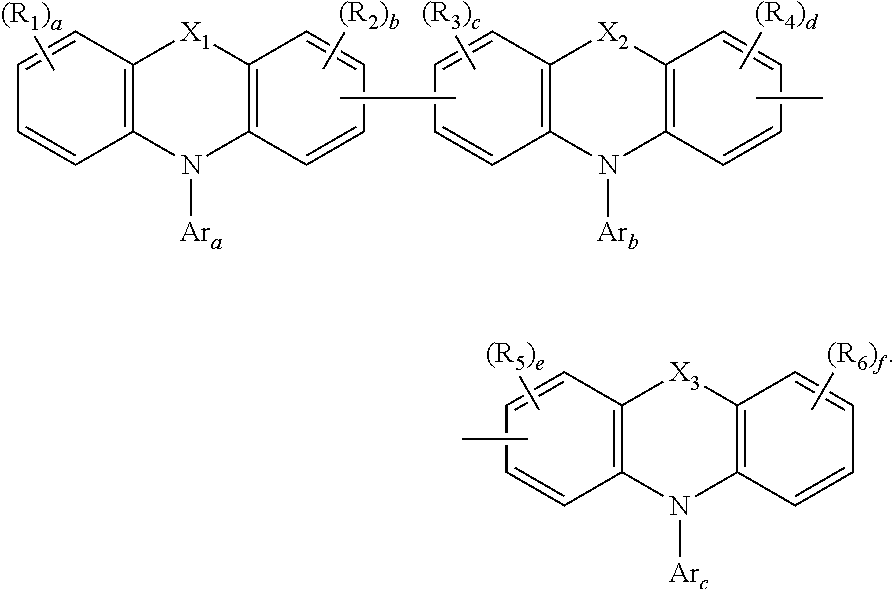
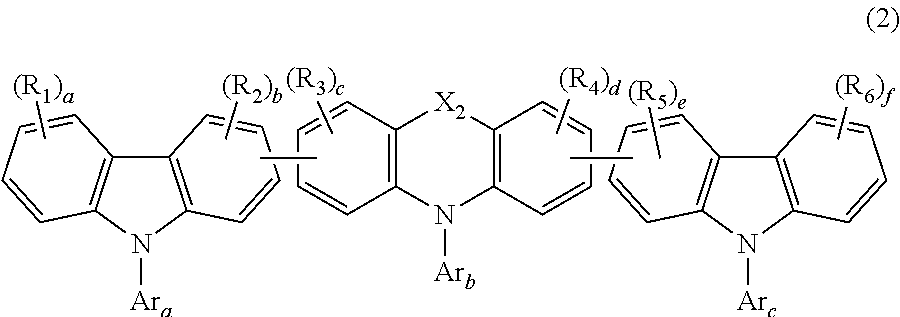
A nitrogen-containing aromatic heterocyclic derivative represented by the following formula, wherein X1 to X3 are a single bond, CRaRb, NRc, an oxygen atom or a sulfur atom, and when all of X1 to X3 is a single bond, at least one of Ara, Arb and Arc is an aryl group having 6 to 20 ring carbon atoms substituted with a heteroaryl group, an aryloxy group or a heteroaryloxy group, or a substituted or unsubstituted heteroaryl group having 5 to 20 ring atoms.

Description

TECHNICAL FIELD[0001]The invention relates to a nitrogen-containing aromatic heterocyclic derivative and an organic electroluminescence device using the same.BACKGROUND ART[0002]An organic electroluminescence device (organic EL device) is a promising solid-state emitting type inexpensive and large full-color display device, and has been extensively developed. In general, an organic EL device includes an emitting layer and a pair of opposing electrodes holding the emitting layer therebetween. When an electric field is applied between the electrodes, electrons are injected from a cathode and holes are injected from an anode. The electrons recombine with the holes in the emitting layer to produce an excited state, and energy is emitted as light when the excited state returns to the ground state.[0003]In addition, a phosphorescent organic EL device has been proposed wherein an organic phosphorescent material is used for an emitting layer of the organic EL device. In the phosphorescent o...

Claims


Application Information

Patent Timeline
IPC IPC(8): H01L51/54C07D403/14C07D401/14C07D405/14
CPCC07D209/86H05B33/14C07D401/14C07D403/14C07D405/14C09K11/06C09K2211/1007C09K2211/1029C09K2211/1033C09K2211/1037C09K2211/1044C09K2211/1088C09K2211/1092H01L51/0059H01L51/0071H01L51/0072H01L51/0085H01L51/5012C07D219/02C09B15/00C09B17/00C09B19/00C09B21/00C09B57/00H10K85/631H10K85/657H10K85/342H10K85/6572H10K50/11H05B33/20
Inventor KATO, TOMOKINISHIMURA, KAZUKIHOSOKAWA, CHISHIONUMATA, MASAKINAGASHIMA, HIDEAKI
Owner IDEMITSU KOSAN CO LTD
Why Eureka
Try Eureka