Eureka AIR delivers breakthrough ideas for toughest innovation challenges, trusted by R&D personnel around the world.

Embedded component device and manufacturing methods thereof

a technology of embedded components and manufacturing methods, applied in the field of embedded components, can solve the problems of increasing the complexity of semiconductor devices, occupying space occupied by both semiconductors, and additional costs incurred by performing packaging, circuit board manufacturing, assembly as separate processes

Active Publication Date: 2012-06-21
ADVANCED SEMICON ENG INC
View PDF9 Cites 101 Cited by
  • Summary
  • Abstract
  • Description
  • Claims
  • Application Information

AI Technical Summary

Problems solved by technology

Semiconductor devices have become progressively more complex, driven at least in part by the demand for smaller sizes and enhanced processing speeds.
This results in space being occupied by both the semiconductor device package and the substrate, and in surface area on the substrate being occupied by the semiconductor device package.
In addition, additional cost may be incurred by performing packaging, circuit board manufacturing, and assembly as separate processes.

Method used


Image

  • Embedded component device and manufacturing methods thereof
  • Embedded component device and manufacturing methods thereof
  • Embedded component device and manufacturing methods thereof

Examples


Embodiment Construction

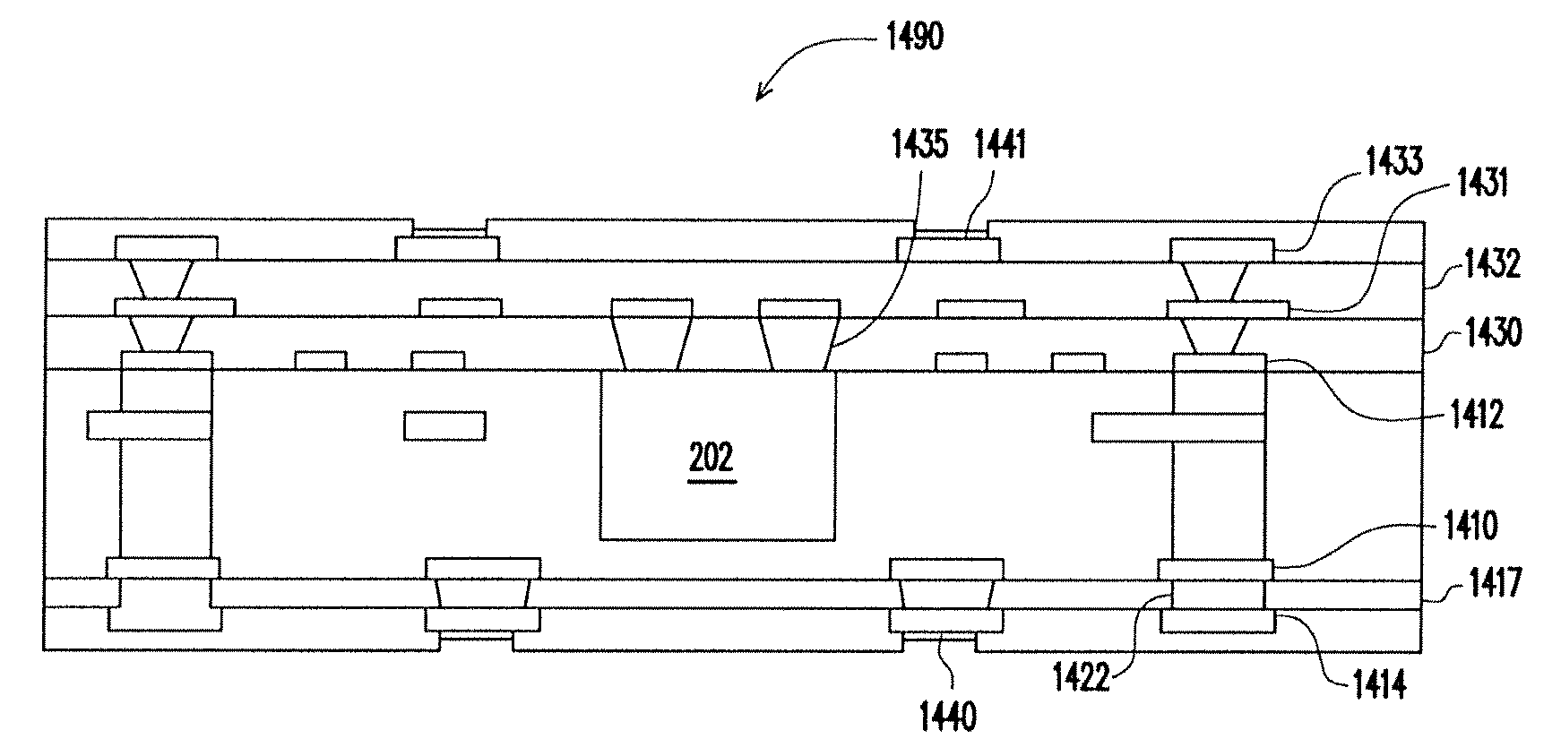
[0025]Attention first turns to FIG. 1, which illustrates a perspective view of an embedded component device 100 implemented in accordance with an embodiment of the invention. The embedded component device 100 may include an embedded package, substrate, and / or module, and may include active components, passive components, or both active and passive components. In the illustrated embodiment, sides of the embedded component device 100 are substantially planar and have a substantially orthogonal orientation so as to define a lateral profile that extends around substantially an entire periphery of the embedded component device 100. This orthogonal lateral profile allows a reduced overall size by reducing or minimizing an area of the embedded component device 100. This reduction in area may be advantageous, for example, because the area may correspond to a footprint area of the embedded component device 100 when stacked on another substrate. However, it is contemplated that the lateral pr...


PUM


Abstract

An embedded component device includes an electronic component including an electrical contact, an upper patterned conductive layer, a dielectric layer between the upper patterned conductive layer and the electronic component, a first electrical interconnect, a lower patterned conductive layer, a conductive via, and a second electrical interconnect. The dielectric layer has a first opening exposing the electrical contact, and a second opening extending from the lower patterned conductive layer to the upper patterned conductive layer. The first electrical interconnect extends from the electrical contact to the upper patterned conductive layer, and fills the first opening. The second opening has an upper portion exposing the upper patterned conductive layer and a lower portion exposing the lower patterned conductive layer. The conductive via is located at the lower portion of the second opening. The second electrical interconnect fills the upper portion of the second opening.

Description

BACKGROUND OF THE INVENTION[0001]1. Field of the Invention[0002]The invention relates generally to substrates including electrical circuitry and manufacturing methods thereof. More particularly, the invention relates to an embedded component device and manufacturing methods thereof.[0003]2. Description of Related Art[0004]Semiconductor devices have become progressively more complex, driven at least in part by the demand for smaller sizes and enhanced processing speeds. At the same time, there is a demand to further miniaturize many electronic products including these semiconductor devices. Semiconductor devices are typically packaged, and then may be installed on a substrate including electrical circuitry, such as a circuit board. This results in space being occupied by both the semiconductor device package and the substrate, and in surface area on the substrate being occupied by the semiconductor device package. In addition, additional cost may be incurred by performing packaging, ...

Claims


Application Information

Patent Timeline
Patent Type & Authority Applications(United States)
IPC IPC(8): H01L23/48H01L21/28
CPCH01L25/16H01L23/5389H01L2924/3025H01L2924/00014H01L2224/73265H01L2224/32225H01L2224/16225H01L2924/01029H01L2224/48227H01L2224/48091H01L24/82H01L24/48H01L24/16H01L24/32H01L2224/24195H01L2224/73267H01L24/24H01L2924/00012H01L2224/45099H01L2924/00H01L2224/04105H01L2924/181H01L24/73H01L2924/15153H01L2224/24227
Inventor LEE, CHUN-CHESU, YUAN-CHANGLEE, MING CHIANGHUANG, SHIH-FU
Owner ADVANCED SEMICON ENG INC
Why Eureka
Eureka Blog
Learn More