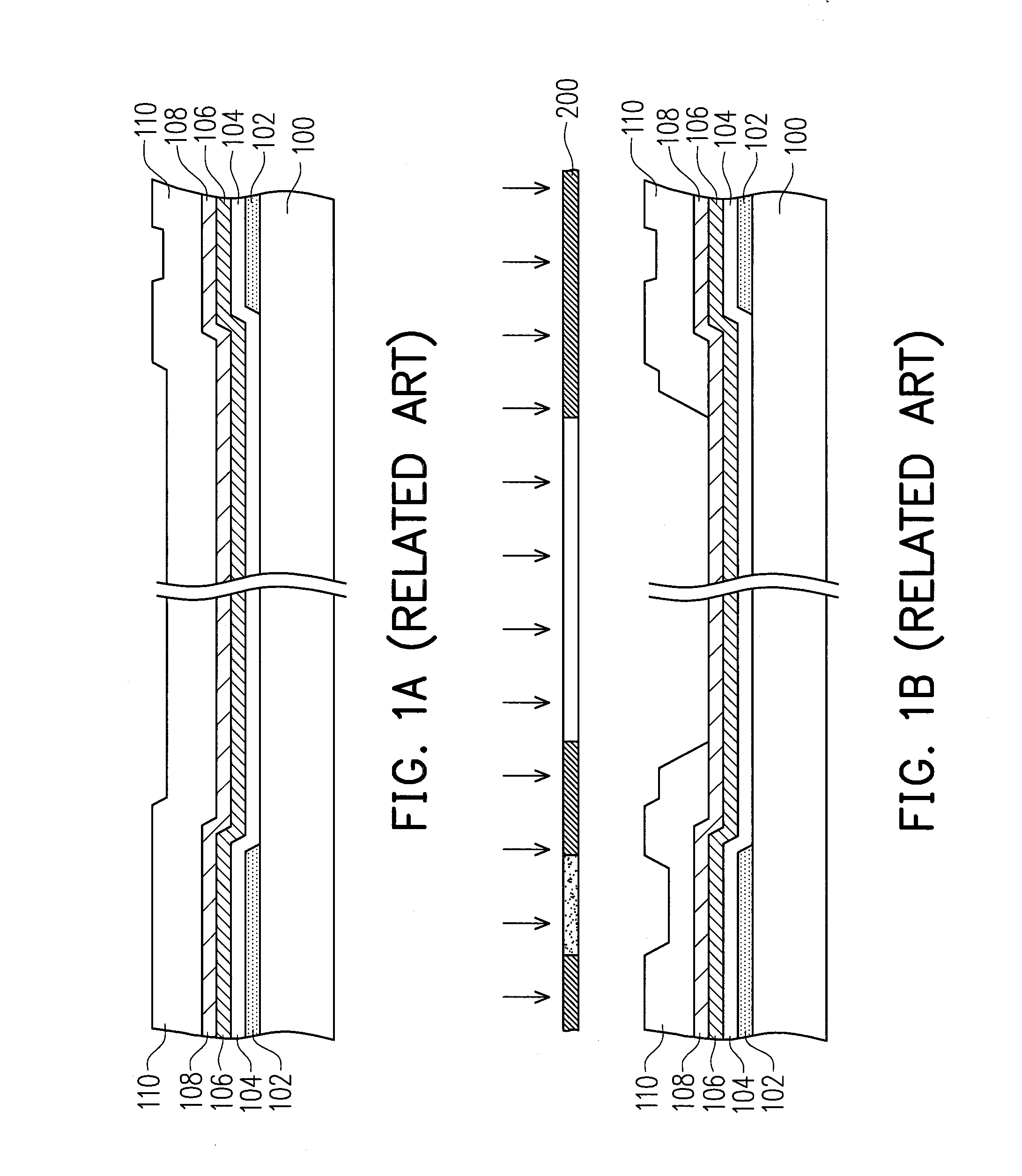
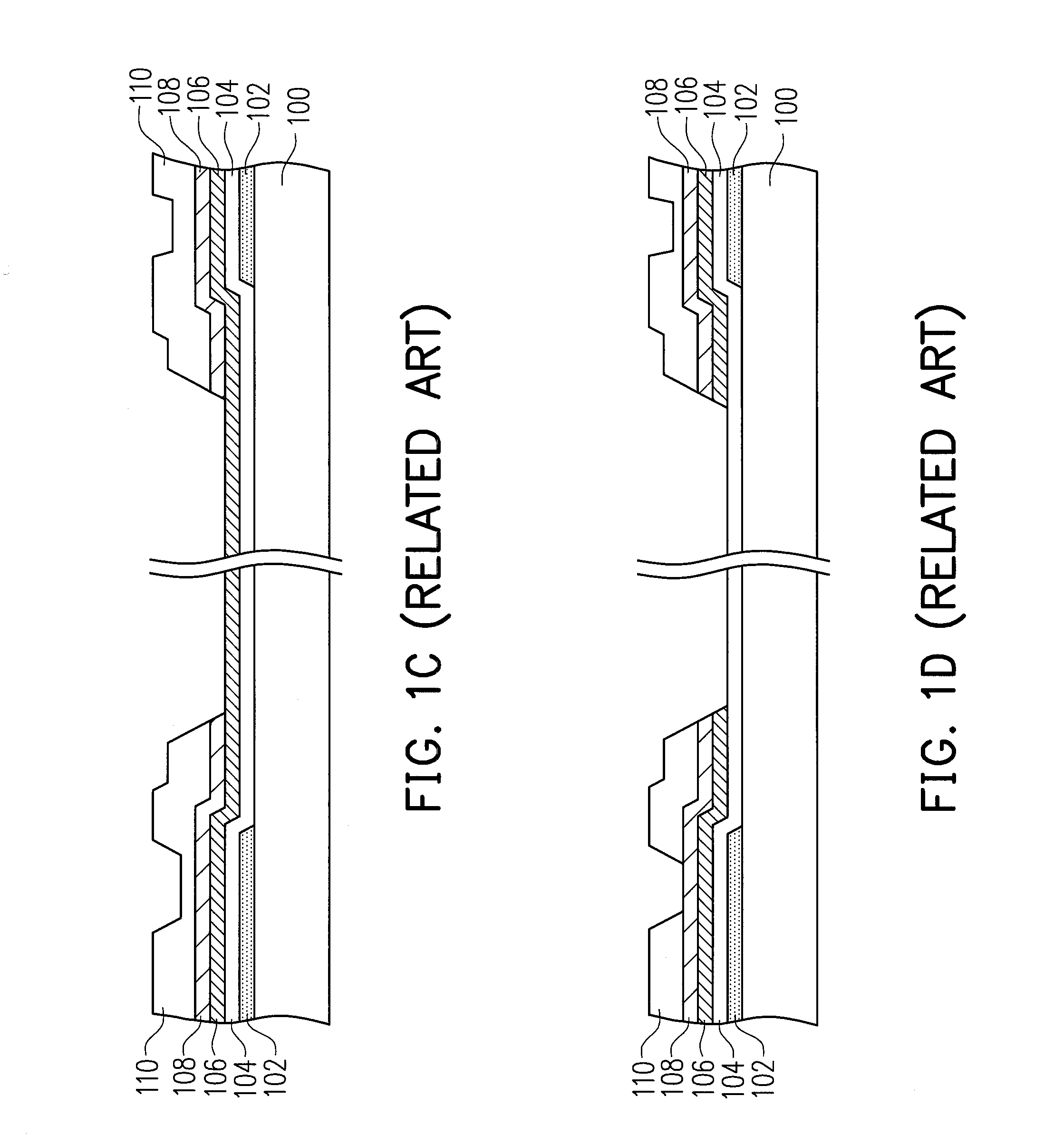
Pixel structure and dual gate pixel structure
a pixel structure and flat panel display technology, applied in semiconductor devices, electrical devices, instruments, etc., can solve the problems of abnormal pixel display, short circuit, and often coated metal layer with non-uniform photoresis
- Summary
- Abstract
- Description
- Claims
- Application Information
AI Technical Summary
Benefits of technology
Problems solved by technology
Method used
Image
Examples
first embodiment
[0031]FIG. 2 is a schematic top view illustrating a pixel structure according to a first embodiment of the invention. FIG. 3A to FIG. 3H are cross-sectional flow charts illustrating a fabrication process of a pixel structure taken along a line I-I′ depicted in FIG. 2. The pixel structure and the fabrication process thereof are elaborated in this embodiment with reference to FIG. 2 and FIG. 3A to FIG. 3H.
[0032]A method of forming the pixel structure in this embodiment is exemplarily described below. As indicated in FIG. 3A, a substrate 300 is provided. A first metal layer 302 is formed on the substrate 300, and a patterning process is performed on the first metal layer 302 with use of the first photo mask. In this embodiment, the patterned first metal layer 302 includes a scan line SL and a common electrode CL separated from the scan line SL. A portion of the scan line SL serves as the gate, as indicated in FIG. 2 and FIG. 3A.
[0033]Note that the common electrode CL of this embodiment...
second embodiment
[0050]The predetermined opening of the common electrode CL as described in the first embodiment is applicable to the dual gate pixel structure of the second embodiment, such that the issue of short circuit between the pixel electrode and the common electrode in the dual gate pixel structure of this embodiment can be prevented as well.
[0051]The method of forming the dual gate pixel structure and the material of each layer in this embodiment are similar to those described in the first embodiment, and thus no further description is provided herein. The difference between the dual gate pixel structure of this embodiment and the pixel structure of the first embodiment is elaborated hereinafter.
[0052]FIG. 4 is a schematic top view illustrating the dual gate pixel structure according to the second embodiment of the invention. The schematic cross-sectional view taken along the sectional lines II-II′ and III-III′ depicted in FIG. 4 is shown in FIG. 3H.
[0053]With reference to FIG. 4 and FIG. ...
PUM
 Abstract
Description
Claims
Application Information
 - R&D
- Intellectual Property
- Life Sciences
- Materials
- Tech Scout
- Unparalleled Data Quality
- Higher Quality Content
- 60% Fewer Hallucinations
Browse by: Latest US Patents, China's latest patents, Technical Efficacy Thesaurus, Application Domain, Technology Topic, Popular Technical Reports.
© 2025 PatSnap. All rights reserved.Legal|Privacy policy|Modern Slavery Act Transparency Statement|Sitemap|About US| Contact US: help@patsnap.com


