
Vertical electrode structure using trench and method for fabricating the vertical electrode structure

a vertical electrode and trench technology, applied in the direction of semiconductor devices, semiconductor/solid-state device details, electrical apparatus, etc., can solve the problems of high process cost, inconvenient large-area electron beam lithography process, and difficulty in manufacturing structures with a size of several hundred nanometers or less, etc., to achieve short processing time and low processing cost

Inactive Publication Date: 2012-04-26
KOREA UNIV RES & BUSINESS FOUND
View PDF4 Cites 4 Cited by
  • Summary
  • Abstract
  • Description
  • Claims
  • Application Information

AI Technical Summary

Benefits of technology

[0010]The present invention is to provide a method of depositing electrodes having a size of several hundreds of nanometers or less and forming the electrodes with a short processing time and a low processing cost.
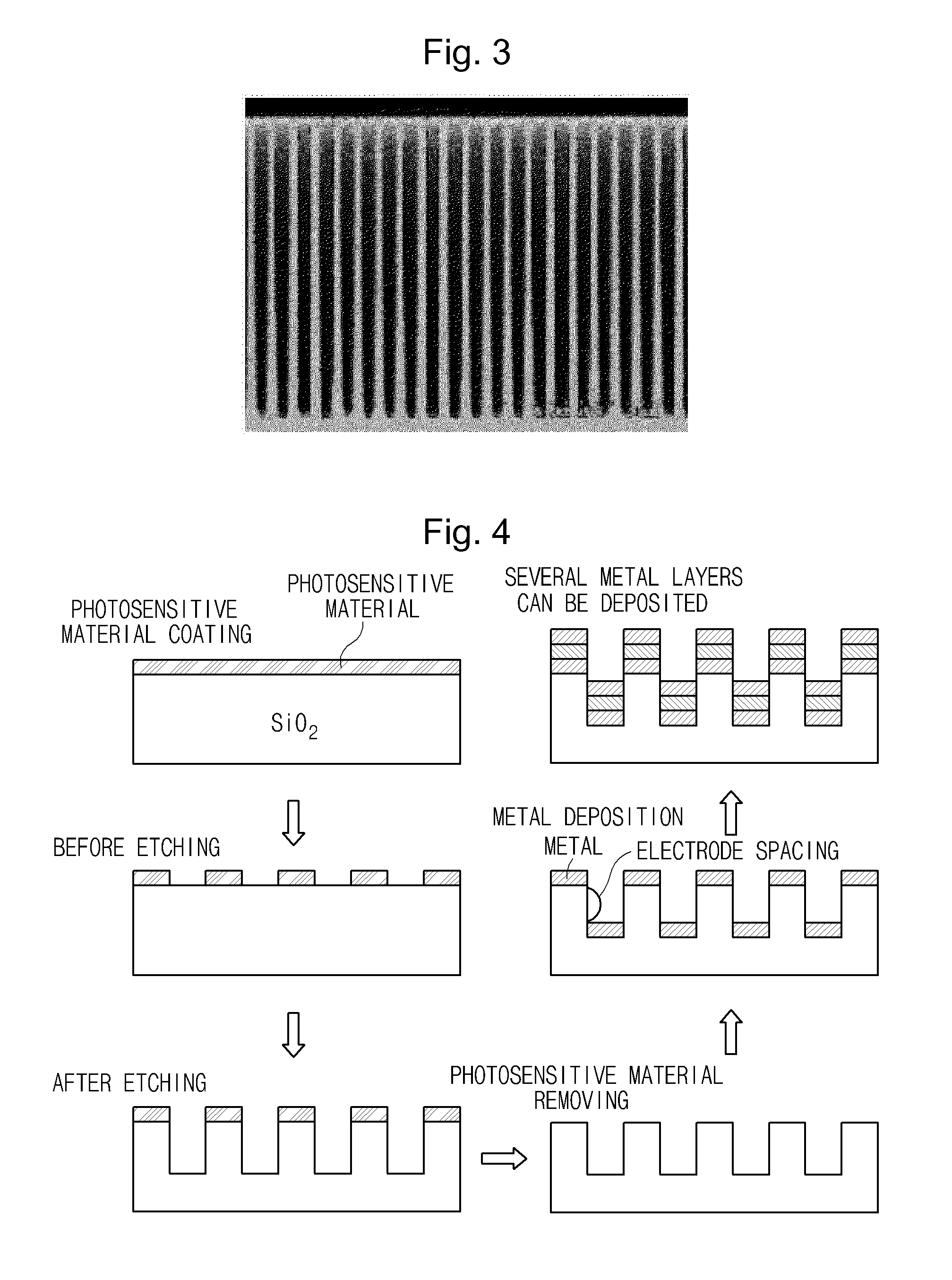
[0012]The electrode layer may be formed by using a deposition process. In this case, a thickness of each of the deposited electrodes is adjusted by controlling an electrode deposition time, so that it is possible to easily adjust an electrode spacing.
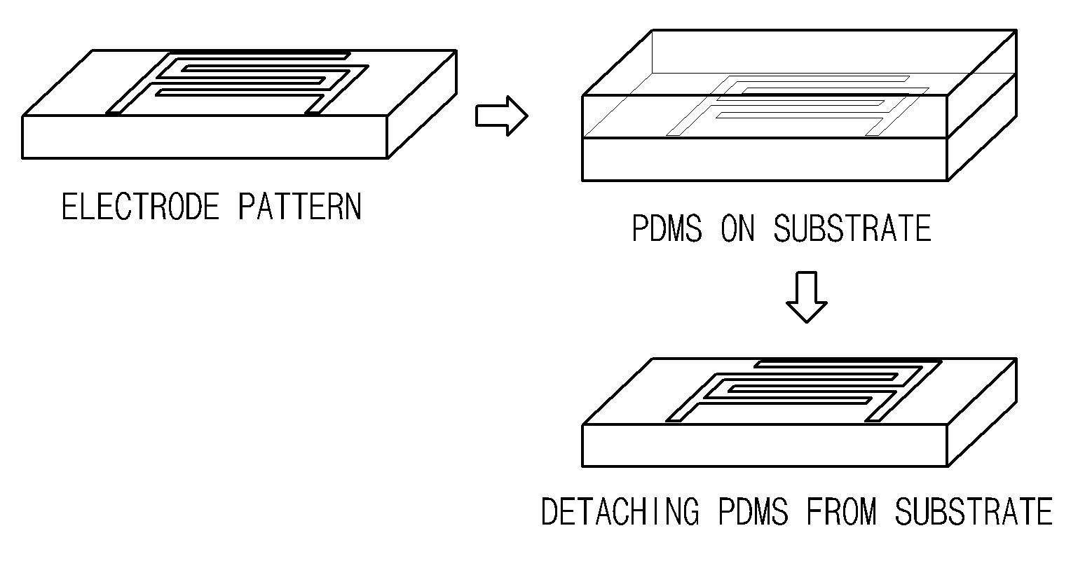
[0015]In addition, the method of forming a vertical electrode structure using a trench may further include steps of: coating a predetermined liquid material on the substrate and curing the liquid material; and detaching the cured material, to which the electrode layer is transferred from the substrate, from the substrate. In this case, the material may be polydimethylsiloxane (PDMS). According to this configuration, it is possible to easily form the vertical electrode structure on the flexible substrate such as PDMS.
[0017]According to the present invention, it is possible to deposit electrodes having a size of several hundreds of nanometers or less with a short processing time and a low processing cost.

Problems solved by technology

However, since the resolution of the photolithography depends on the wavelength of UV light, there is a problem in that, although a structure having a size of several micrometers (um) can be manufactured, it is difficult to manufacture a structure having a size of several hundreds of nanometers (nm) or less.
However, since a long processing time is taken and the process cost is high, the electron beam lithography process is not suitable for a large-area process.

Method used


Image

  • Vertical electrode structure using trench and method for fabricating the vertical electrode structure
  • Vertical electrode structure using trench and method for fabricating the vertical electrode structure
  • Vertical electrode structure using trench and method for fabricating the vertical electrode structure

Examples


Embodiment Construction

[0026]Hereinafter, preferred embodiments of the present invention will be described with reference to the attached drawings.

[0027]FIG. 2 is a schematic flowchart illustrating a vertical electrode structure forming method using a trench according to an embodiment of the present invention.

[0028]In FIG. 2, first, the trench is formed in a pre-defined region of a semiconductor substrate (S110). Herein, the predetermined region denotes a region on the semiconductor substrate, which is defined in advance by a semiconductor designer or the like in order to form the trench.

[0029]As described in the Background Art, the problems occur because the electrodes are arrayed parallel to the direction of the substrate. If the electrodes are designed to be arrayed perpendicular to the direction of the substrate, it is possible to avoid difficulty in the process.

[0030]In order to a vertical electrode, the trench structure may be used. A typical trench structure is illustrated in FIG. 3. FIG. 3 is a vi...


PUM


Abstract

Provided is a vertical electrode structure using a trench and a method of manufacturing the vertical electrode structure. The method of forming a vertical electrode structure using a trench includes steps of: forming the trench on a predetermined region of a semiconductor substrate; and forming electrode layers in predetermined regions of inner and outer portions of the trench. In this manner, the electrode deposition in the vertical direction is established by using the trench, so that it is possible to form a deposited electrode having a size of several hundred nm or less by a short processing time and a low processing cost.

Description

BACKGROUND OF THE INVENTION[0001]1. Field of the Invention[0002]The present invention relates to a semiconductor device structure and, more particularly, to an electrode structure in a semiconductor device.[0003]2. Description of the Related Art[0004]In an article disclosed in Biosensors and Bioelectronics in 2009, it is known that, if the electrode spacing is decreased and the number of electrodes is increased, reaction sensitivity is increased. A capacitance of an element is defined by C=εA / d. As the number of electrodes is increased, the total area A of electrode is increased. As the electrode spacing is decreased, the total capacitance is increased.[0005]In terms of resistance, as the cross section of the channel through which a current can be flowed is increased and the length of the channel is decreased, the value of resistance is decreased. The amount of the measured current may be increased.[0006]In the conventional technology, in order to obtain this effect, an interdigitat...

Claims


Application Information

Patent Timeline
IPC IPC(8): H01L23/48H01L21/768
CPCH01L23/4824B81C1/00166H01L2924/00013H01L24/06H01L2224/13099H01L2224/13599H01L2224/05599H01L2224/05099H01L2224/29099H01L2224/29599H01L2924/01322H01L2924/00
Inventor KIM, GYU-TAEPARK, SO-JEONGJEON, DAE-YOUNGKIM, YUN-JEONG
Owner KOREA UNIV RES & BUSINESS FOUND
Learn More