Bipolar transistor
- Summary
- Abstract
- Description
- Claims
- Application Information
AI Technical Summary
Problems solved by technology
Method used
Image

Examples
first embodiment
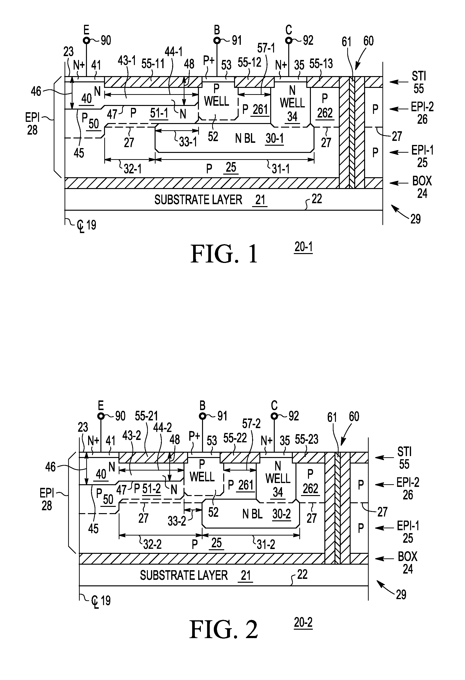
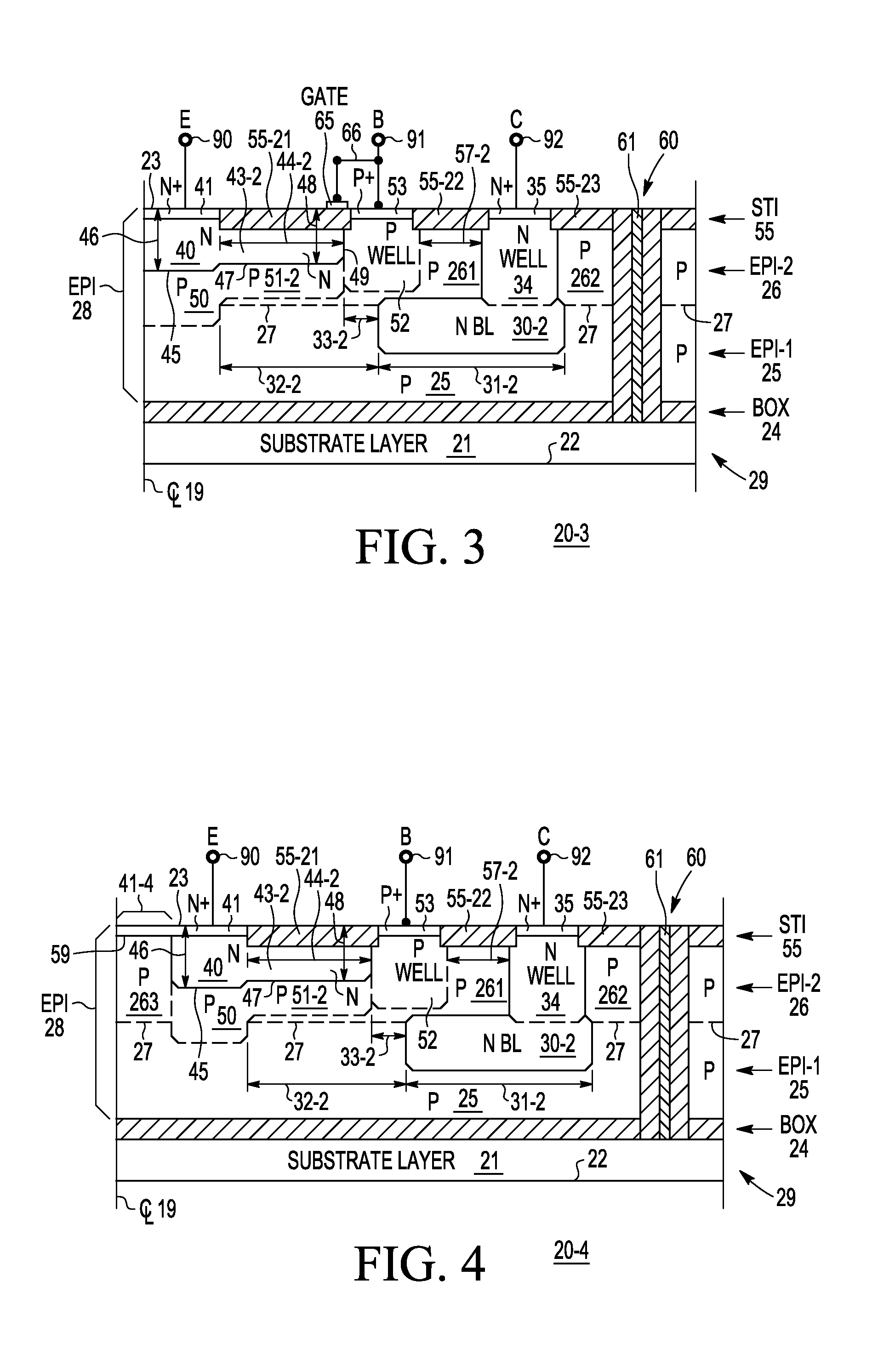
[0037] there is provided a bipolar transistor (20), comprising, a semiconductor substrate (29) having a first surface (23), a first emitter region (40) of a first conductivity type in the semiconductor substrate (29) having a first emitter region doping concentration, a first base region (50) of a second, opposite, conductivity type in the semiconductor substrate (29) underlying the first emitter region (40, 41-4) and having a first base region doping concentration, the first base region (50) forming a first PN or NP junction (45, 59) with the first emitter region (40) at a first depth (46) from the first surface (23), a second emitter region (43) of the first conductivity type in the semiconductor substrate (29) having a second emitter region doping concentration and Ohmically coupled to the first emitter region (40), a second base region (51) of the second conductivity type in the semiconductor substrate (29) underlying the second emitter region (43) and having a second base regio...
second embodiment
[0038] there is provided a method for forming a bipolar transistor, comprising, providing a semiconductor containing substrate (29) with an upper surface (23), and having therein a buried layer collector region (30) of a first conductivity type located below the upper surface (23) and of a buried layer collector region doping concentration, wherein a first portion (25) of the substrate located below the buried layer collector region (30) and a second portion (26) of the substrate located above the buried layer collector region (30) are of a second, opposite, conductivity type, forming during one or more first doping steps in the second portion (26) of the substrate (29), first (40) and second (43) adjacent emitter regions of the first conductivity type near the first surface, the first emitter region extending substantially to the first surface and laterally separated from the buried layer collector region (30), and forming during one or more second doping steps in the second portio...
third embodiment
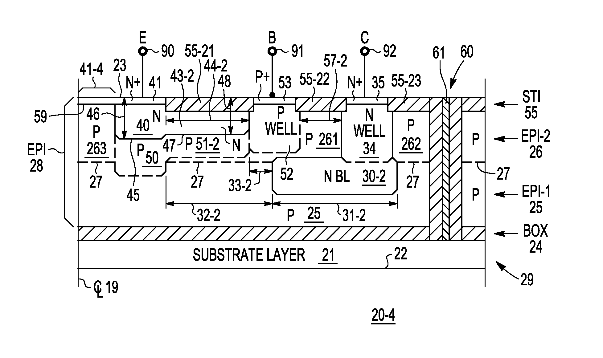
[0039] there is provided a bipolar transistor (20) having a first surface (23), comprising, first (45) and second (47) connected emitter-base junctions having, respectively, first (46) and second (48) different junction depths beneath the first surface (23), and a buried layer collector region (30) having a third depth (304) beneath the first surface (23), the third depth (304) being greater than the first (46) or second (48) depths, wherein the buried layer collector region (30) does not underlie the first (45) emitter-base junction. According to a further embodiment, the buried layer collector region (30) underlies at least a portion of the second emitter-base junction (47). According to a still further embodiment, the transistor (20) further comprises an isolation region (55-11, 55-21) overlying the second emitter-base junction (47) but not overlying the first emitter-base junction (45). According to a yet further embodiment, the transistor (20) still further comprises a conducti...
PUM
 Abstract
Description
Claims
Application Information
 - R&D
- Intellectual Property
- Life Sciences
- Materials
- Tech Scout
- Unparalleled Data Quality
- Higher Quality Content
- 60% Fewer Hallucinations
Browse by: Latest US Patents, China's latest patents, Technical Efficacy Thesaurus, Application Domain, Technology Topic, Popular Technical Reports.
© 2025 PatSnap. All rights reserved.Legal|Privacy policy|Modern Slavery Act Transparency Statement|Sitemap|About US| Contact US: help@patsnap.com