Memory Device and Read Operation Method Thereof
a memory device and read operation technology, applied in information storage, static storage, digital storage, etc., can solve the problems of reducing the read margin of sensing erase cells, circuit area and current consumption become important issues, etc., and achieve the effect of reducing the setup time of signal lines in page read
- Summary
- Abstract
- Description
- Claims
- Application Information
AI Technical Summary
Benefits of technology
Problems solved by technology
Method used
Image
Examples
first embodiment
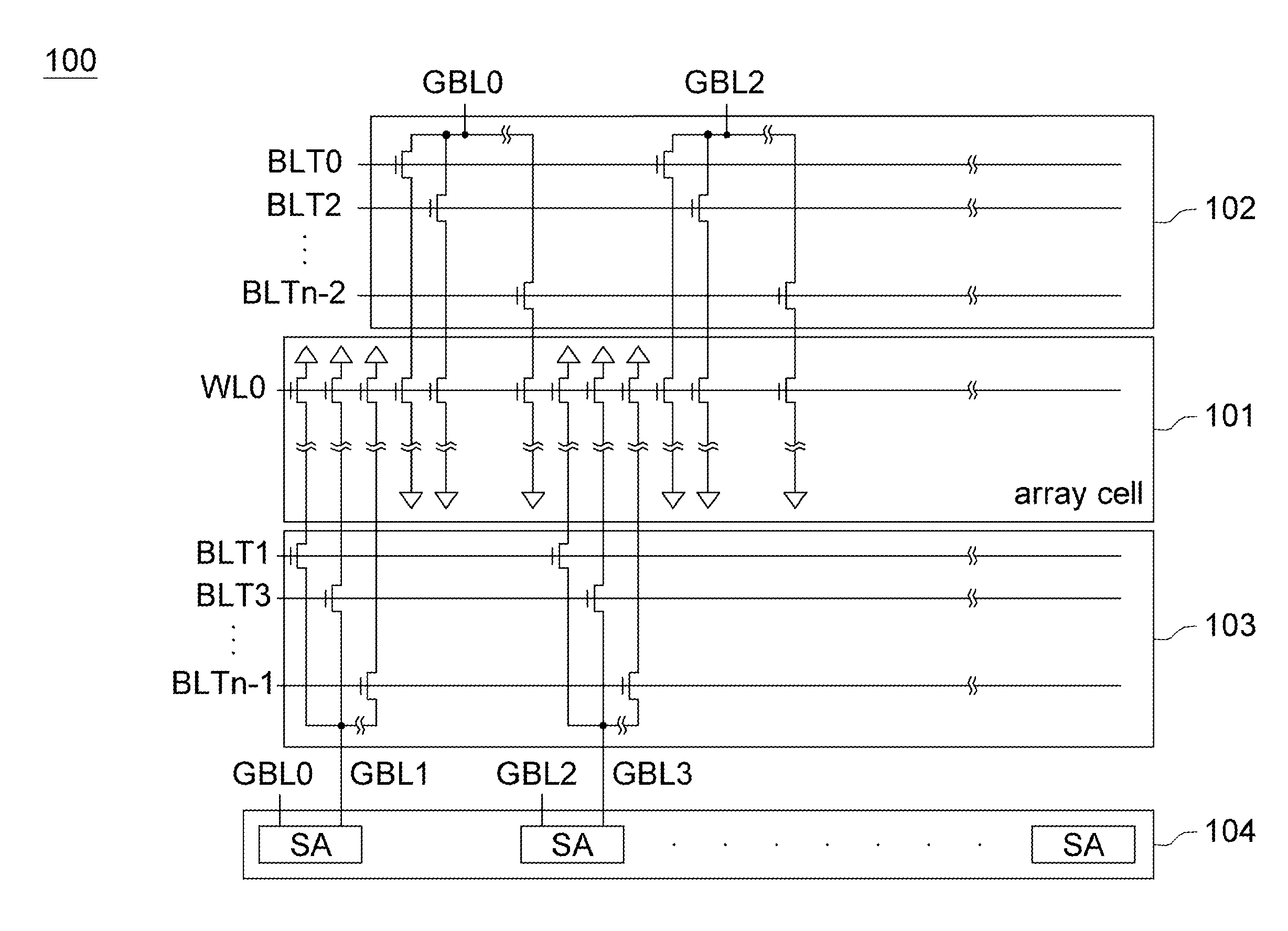
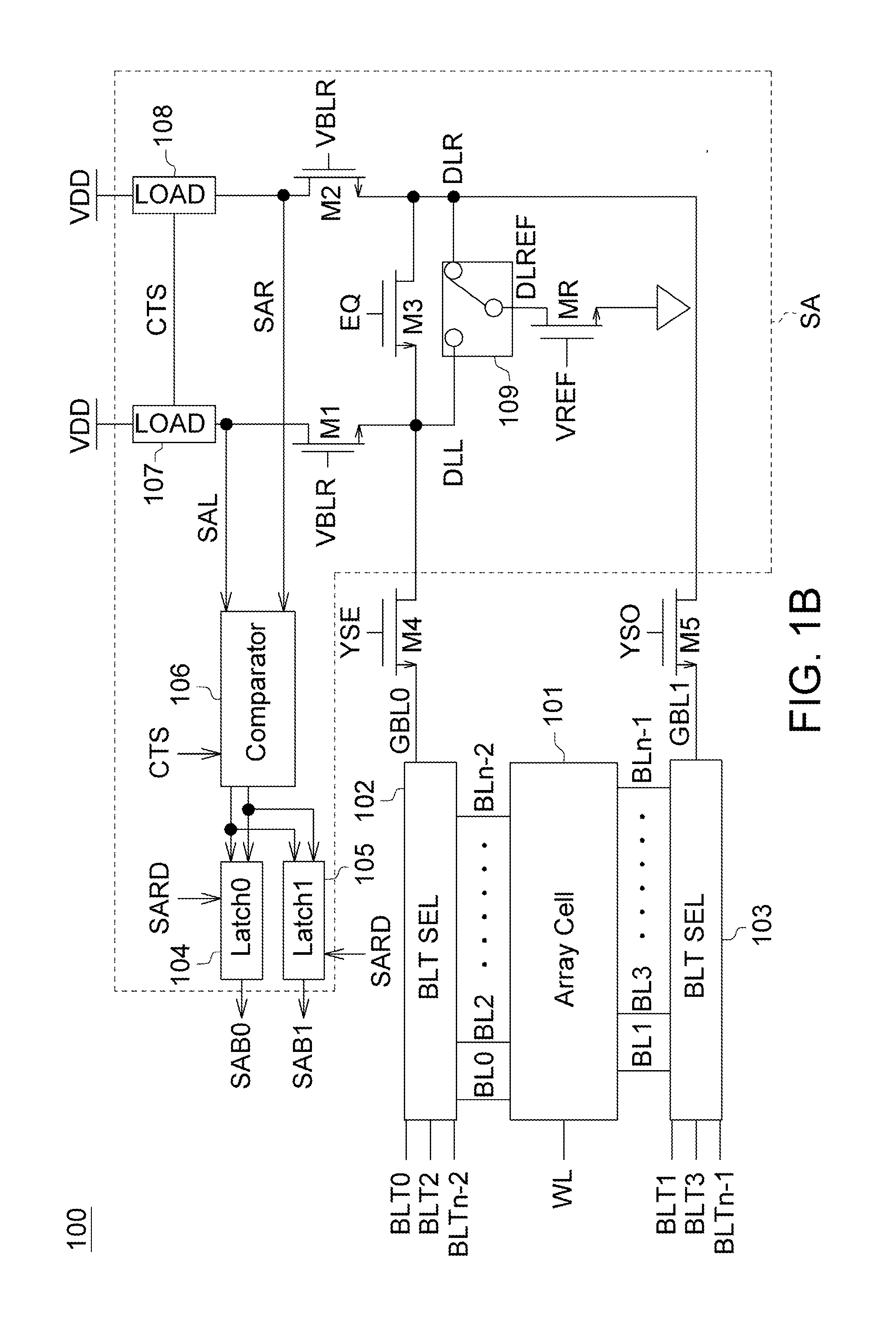
[0016]FIG. 1A shows a simplified diagram and FIG. 1B shows a function block diagram of a memory device according to a first embodiment of the disclosure. As shown in FIG. 1A, the memory device100 according to the first embodiment of the disclosure at least includes an array cell 101, bit line selectors 102˜103 and a sensing amplifier circuit 104. The array cell 101 has a plurality of memory cells arranged in an array. The bit line selector 102 includes a plurality of bit line selection transistors for selectively conducting the global bit lines GBL0, GBL2 . . . to the array cell 101 according to the bit line selection signals BLT0, BLT2 . . . BLTn-2. Similarly, the bit line selector 103 includes a plurality of bit line selection transistors for selectively conducting the global bit lines GBL1, GBL 3 . . . to the array cell 101 according to the bit line selection signals BLT1, BLT3 . . . BLTn-1. The sensing amplifier circuit 104 has a plurality of sensing amplifiers SA. Each SA in th...
second embodiment
[0034]FIG. 5 shows a function block diagram of a memory device according to a second embodiment of the disclosure. As shown in FIG. 5, the memory device 500 according to the second embodiment of the disclosure at least includes an array cell 501, bit line selectors 502˜503 and a sensing amplifier circuit (not shown). The SA includes latches 504˜505, a comparator 506, loads 507A˜508B, a reference side selector 509, multiplexers 510˜513 and transistors MR, M1A˜M3B. The array cell 501, the bit line selectors 502˜503, the latches 504˜505, the comparator 506, the loads 507A˜508B, the reference side selector 509 and the transistors MR, M1A˜M5B are the same or similar to that in the first embodiment and thus their details are omitted. The control signal A3 controls the MUXs 510˜513 for the first half page reading and for the second half page reading.
[0035]The timing waveform of the second embodiment 500 of the disclosure is shown in FIG. 6.
[0036]At the WL / GBL / BL setup phase, the control si...
third embodiment
[0042]FIG. 7 shows a function block diagram of a memory device according to a third embodiment of the disclosure. As shown in FIG. 7, the memory device 700 according to the third embodiment of the disclosure at least includes an array cell 701, bit line selectors 702˜703 and a sensing amplifier circuit (not shown). The SA includes latches 704˜705, a comparator 706, loads 707A˜708, a reference side selector 709, multiplexers 710˜712 and transistors MR, M1A˜M3B. The SA in the third embodiment has similar structure and operation to that in the second embodiment and thus the details are omitted. The control signal A6 controls the reference side selector 709 and the multiplexers 711˜712. During read operation, the signals YES0 and YEO0 are both high. If the control signal is L, the node DLL0 is connected to the global bit line GBL0 via the MUX 712; the node DLL1 is connected to the global bit line GBL2 via the MUX 711; and the node DLREF is connected to the global bit line GBL1 via the r...
PUM
 Abstract
Description
Claims
Application Information
 - R&D
- Intellectual Property
- Life Sciences
- Materials
- Tech Scout
- Unparalleled Data Quality
- Higher Quality Content
- 60% Fewer Hallucinations
Browse by: Latest US Patents, China's latest patents, Technical Efficacy Thesaurus, Application Domain, Technology Topic, Popular Technical Reports.
© 2025 PatSnap. All rights reserved.Legal|Privacy policy|Modern Slavery Act Transparency Statement|Sitemap|About US| Contact US: help@patsnap.com


