
Solid-state imaging device and method for manufacturing the same

a solid-state imaging and manufacturing method technology, applied in semiconductor devices, radio frequency controlled devices, electrical devices, etc., can solve the problems of color mixing, lowering the sensitivity to red light, and color mixing, so as to reduce the sensitivity, reduce the sensitivity, and reduce the sensitivity. , the effect of reducing the sensitivity

Inactive Publication Date: 2012-02-09
SONY CORP
View PDF4 Cites 1 Cited by
  • Summary
  • Abstract
  • Description
  • Claims
  • Application Information

AI Technical Summary

Benefits of technology

The present invention provides a solid-state imaging device and a method for manufacturing it that can enhance sensitivity to red light. The device includes a reflective surface that is formed inside or under a charge accumulation region and is designed to reflect light that has passed through the charge accumulation region and direct it toward the center part of the charge accumulation region. This helps to focus the light and improve sensitivity. The method includes steps of forming recesses in a silicon layer, forming a reflective film on the surface of the silicon layer, etching the reflective film, and forming a second silicon layer in a way that preserves the reflective film. The invention also provides a method for manufacturing a solid-state imaging device that includes a hole that is substantially perpendicular to the surface of the silicon layer and has a concave surface as its bottom surface, and a reflective film formed on the surface of the silicon layer and the surface of the concave surface.

Problems solved by technology

This leads to the lowering of the sensitivity to red light.
The light that has gotten out of the photodiode region often enters an adjacent pixel and causes color mixing.
Moreover, a method for forming the reflective film under the photodiode is not disclosed in Patent Document 1, and therefore how the reflective film is formed under the photodiode is unclear.

Method used


Image

  • Solid-state imaging device and method for manufacturing the same
  • Solid-state imaging device and method for manufacturing the same
  • Solid-state imaging device and method for manufacturing the same

Examples


first embodiment

2. Structure and Manufacturing Method of First Embodiment of Present Invention

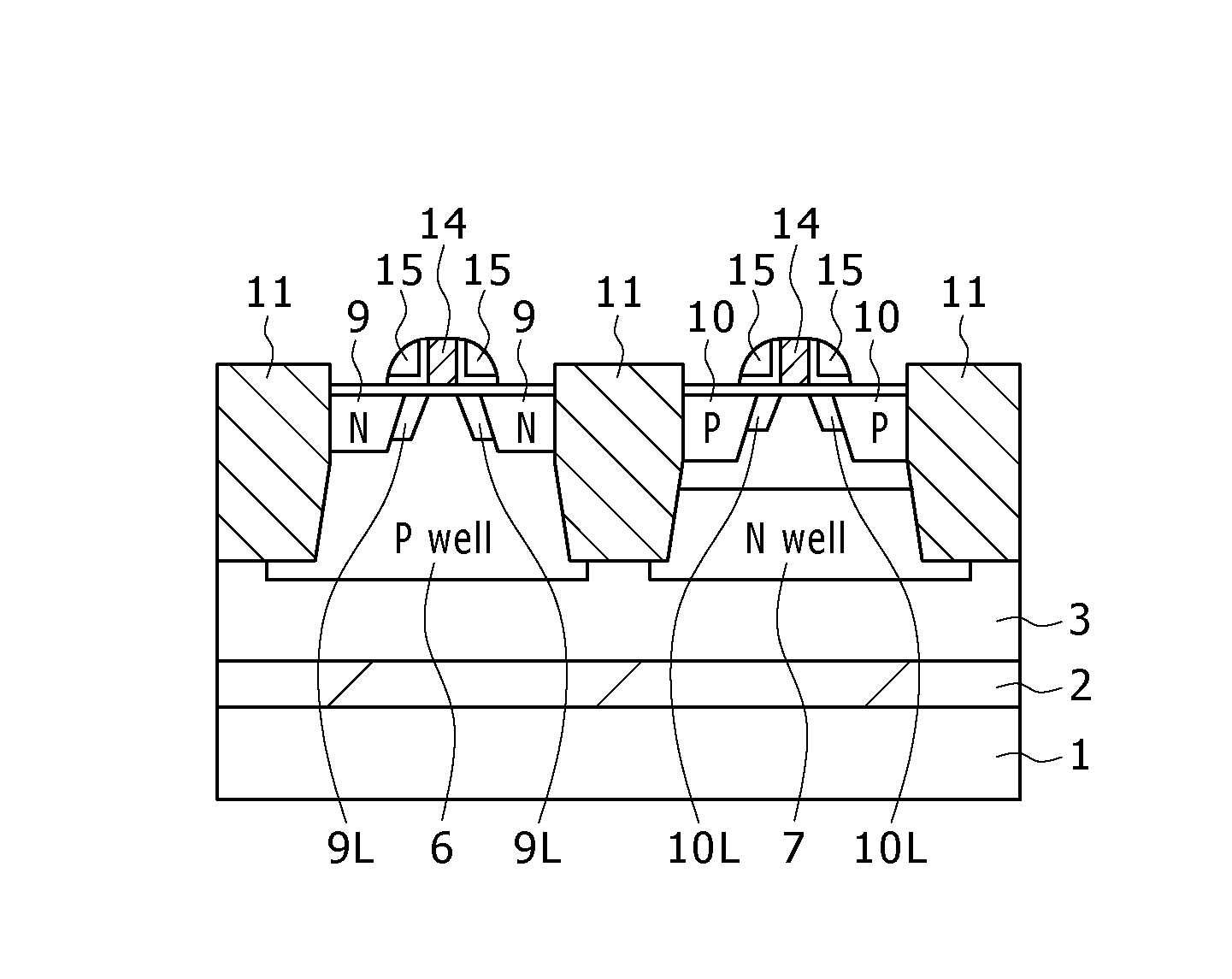
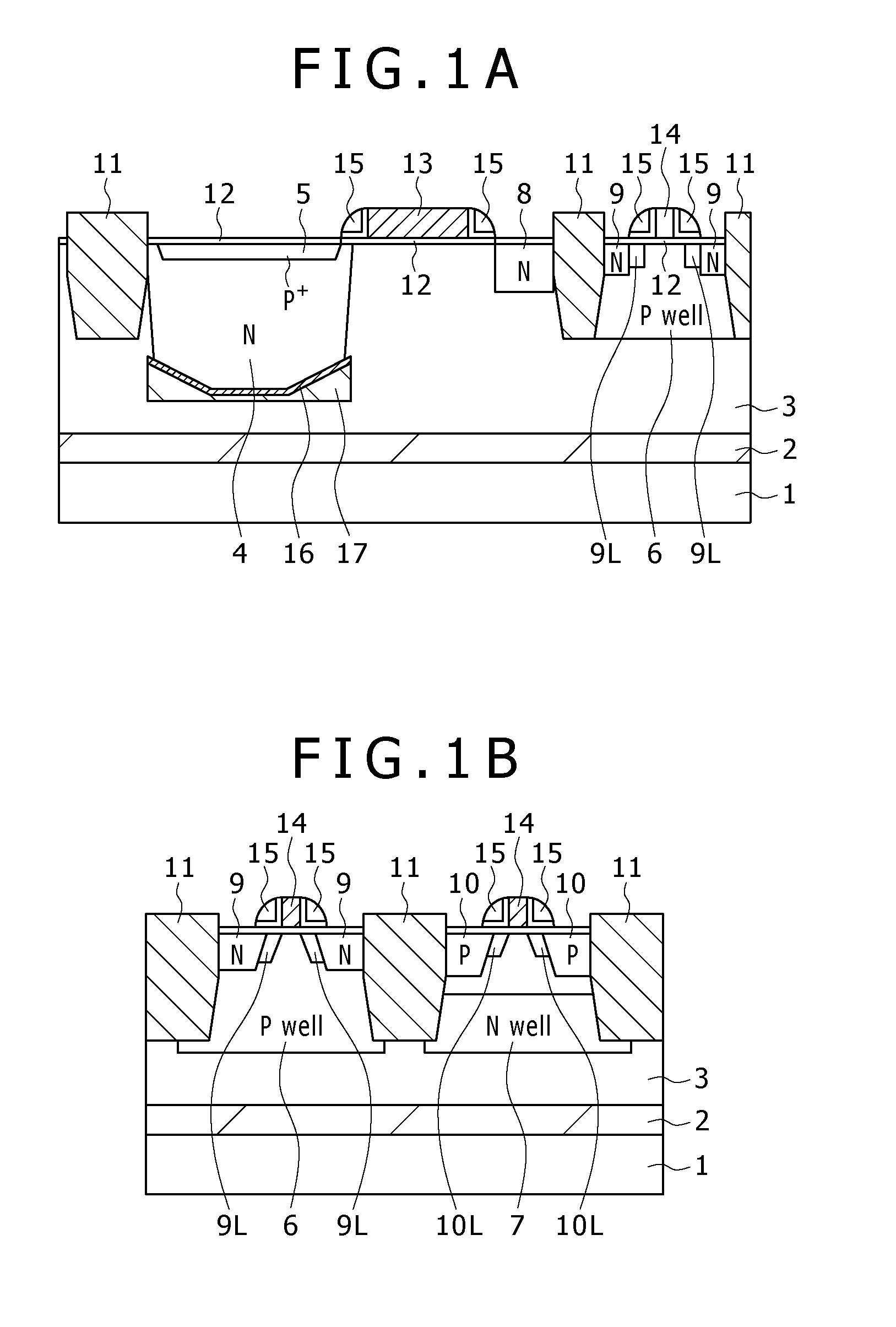
[0127]FIGS. 1A and 1B are schematic structural diagrams (sectional views) of a solid-state imaging device according to a first embodiment of the present invention. FIG. 1A is a sectional view of the pixel area, and FIG. 1B is a sectional view of the peripheral circuit part. The present embodiment is application to a CMOS sensor (CMOS solid-state imaging device).

[0128]As shown in FIGS. 1A and 1B, a base is formed by stacking a silicon substrate 1, a silicon oxide layer 2, and a silicon layer 3 in that order, and photodiodes, transistors, and so on included in the pixels and the peripheral circuits are formed inside and on the silicon layer 3.

[0129]In the pixel area shown in FIG. 1A, an N-type charge accumulation region 4 is formed inside the silicon layer 3 as a region included in a photodiode serving as a light-receiving part. A P-type (P+) hole accumulation region 5 is formed in the vicinity of the surfac...

second embodiment

3. Structure and Manufacturing Method of Second Embodiment of Present Invention

[0208]FIG. 13 is a schematic structural diagram (sectional view) of a solid-state imaging device according to a second embodiment of the present invention. The present embodiment is also application to a CMOS sensor (CMOS solid-state imaging device).

[0209]As shown in FIG. 13, a base is formed by stacking a silicon substrate 41, an insulating layer 42, and a silicon layer 45 in that order.

[0210]Photodiodes 46 are formed as light-receiving parts inside the silicon layer 45.

[0211]Adjacent to the photodiode 46, a readout gate electrode composed of a gate electrode 48 and a sidewall insulating layer 49 on the sidewall of the gate electrode 48 is formed.

[0212]A thin gate insulating film 47 is formed between the silicon layer 45 and the readout gate electrodes.

[0213]In the photodiode 46 as the light-receiving part, the charge accumulation region 4 and the hole accumulation region 5 shown in FIG. 1A are formed al...


PUM


Abstract

A solid-state imaging device including: a semiconductor layer; a charge accumulation region configured to be formed inside the semiconductor layer and serve as part of a photodiode; and a reflective surface configured to be disposed inside or under the charge accumulation region and be so formed as to reflect light that has passed through the charge accumulation region and direct the light toward a center part of the charge accumulation region.

Description

RELATED APPLICATION DATA[0001]This application is a continuation of U.S. patent application Ser. No. 12 / 545,924, filed Aug. 24, 2009, the entirety of which is incorporated herein by reference to the extent permitted by law. The present application claims the benefit of priority to Japanese Patent Application No. JP 2008-217255 filed in the Japan Patent Office on Aug. 26, 2008, the entirety of which is incorporated by reference herein to the extent permitted by law.BACKGROUND OF THE INVENTION[0002]1. Field of the Invention[0003]The present invention relates to a solid-state imaging device and a method for manufacturing the same.[0004]2. Description of the Related Art[0005]For a solid-state imaging device such as a CMOS (complementary metal oxide semiconductor) sensor (CMOS solid-state imaging device), the potential design for defining the charge accumulation region of the photodiode in each pixel is becoming difficult as the miniaturization of the pixels progresses.[0006]The reasons ...

Claims


Application Information

Patent Timeline
Patent Type & Authority Applications(United States)
IPC IPC(8): H01L31/0232H01L21/02H01L21/20H01L27/12H01L27/14H01L27/146
CPCH01L27/14603H01L27/146
Inventor IKEDA, HARUMINAKAZAWA, MASASHI
Owner SONY CORP
Learn More