
Photovoltaic cell manufacturing method and photovoltaic cell manufacturing apparatus

Inactive Publication Date: 2012-01-19
ULVAC INC
View PDF4 Cites 3 Cited by
  • Summary
  • Abstract
  • Description
  • Claims
  • Application Information

AI Technical Summary

Benefits of technology

[0038]According to the photovoltaic cell manufacturing method of the present invention, the position of the scribing line is specified based on the image data obtained by the image-capturing device in an image analyzing device, and it is possible to accurately determine the position on the compartment element which is irradiated with laser light with reference to laser light irradiation position data that are stored in advance.
[0039]In a conventional case, since movement of the stage on which a photovoltaic cell is mounted is controlled with reference to an alignment mark provided at the periphery of the substrate or an edge portion (end portion) of the substrate, an extremely expensive stage has been necessary which is capable of transferring the photovoltaic cell by a micro distance such as several μm after the large-scale photovoltaic cell having a length of several meters is moved by, for example, one meter.
[0040]In contrast, according to the present invention, after the substrate is preliminarily transferred such that a rough position at which a structural defect exists corresponds to the position of the image-capturing device, the image-capturing device captures the region in which the structural defect exists; the distance between the structural defect and the scribing line which is closest to the structural defect is calculated based on the image data obtained by the image-capturing device in the image analyzing device, and the position of the stage is controlled. Because of this, it is not necessary to use an expensive stage which can, for example, control with a high level of precision in a wide range of, for example, several μm to several meters.
[0041]For this reason, it is possible to accurately and electrically separate (remove) a structural defect by use of a low cost stage. Additionally, according to the photovoltaic cell manufacturing apparatus of the present invention, after the substrate is preliminarily transferred such that a rough position at which a structural defect exists corresponds to the position of the image-capturing device, the image-capturing device captures the region in which the structural defect exists; the distance between the structural defect and the scribing line which is closest to the structural defect is calculated based on the image data obtained by the image-capturing device in the image analyzing device, and the position of the stage is controlled.
[0042]Because of this, it is not necessary to use an expensive stage which can, for example, control with a high level of precision.
[0043]For this reason, it is possible to accurately and electrically separate (remove) a structural defect by use of a low cost stage.

Problems solved by technology

However, in contrast, in the photovoltaic cell in which the silicon single crystal is utilized, a silicon single crystal ingot is sliced, and a sliced silicon wafer is used in the photovoltaic cell; therefore, a large amount of energy is spent for manufacturing the ingot, and the manufacturing cost is high.
Specifically, at the moment, in a case of realizing a photovoltaic cell having a large area which is placed out of doors or the like, when the photovoltaic cell is manufactured by use of a silicon single crystal, the cost considerably increases.
In the amorphous silicon photovoltaic cell that is provided with a photoelectric converter constituted of the foregoing upper and lower electrodes and the semiconductor film, the difference in the electrical potentials is small if each of the layers having a large area is only uniformly formed on the substrate, and there is a problem in that the resistance increases.
However, in the amorphous silicon photovoltaic cell having the foregoing structure, it is known that several structural defects occur during a manufacturing step therefor.
In the photoelectric converter as mentioned above, when structural defects occur such that the upper electrode and the lower electrode are locally short-circuited with the semiconductor film interposed therebetween, the defects cause malfunctions such that power generation voltage or photoelectric conversion efficiency are degraded.
A transfer stage, for example, on which a large-scale photovoltaic cell having a size exceeding one meter is mounted, and in which the movement precision of approximately several tens μm is maintained, is extremely expensive, and there is thereby a concern that the cost of manufacturing large-scale photovoltaic cells in high-volume production significantly increases.

Method used


Image

  • Photovoltaic cell manufacturing method and photovoltaic cell manufacturing apparatus
  • Photovoltaic cell manufacturing method and photovoltaic cell manufacturing apparatus
  • Photovoltaic cell manufacturing method and photovoltaic cell manufacturing apparatus

Examples


modified example

[0139]Next, a modified example of the above-described embodiment will be specifically described.

[0140]In the above-described embodiment, the image-capturing device 32 modulates the magnification ratio, captures the region including the structural defect D and the scribing line 19, and obtains the image (region image) including the scribing line image and the structural defect image.

[0141]In this case, a reference distance is unclear in the image.

[0142]In the modified example, firstly, an image reference point in the image (for example, center point) is set.

[0143]In other cases, the image reference point may be determined in advance so as to be a constant position in the image at all times.

[0144]Additionally, the image reference point may be optionally determined in the image.

[0145]The point on the substrate corresponding to the image reference point when the image is obtained at the time of capturing is a substrate reference point.

[0146]Next, due to an image processing, the position...


PUM

PropertyMeasurementUnit
Ratioaaaaaaaaaa
Distanceaaaaaaaaaa

Abstract

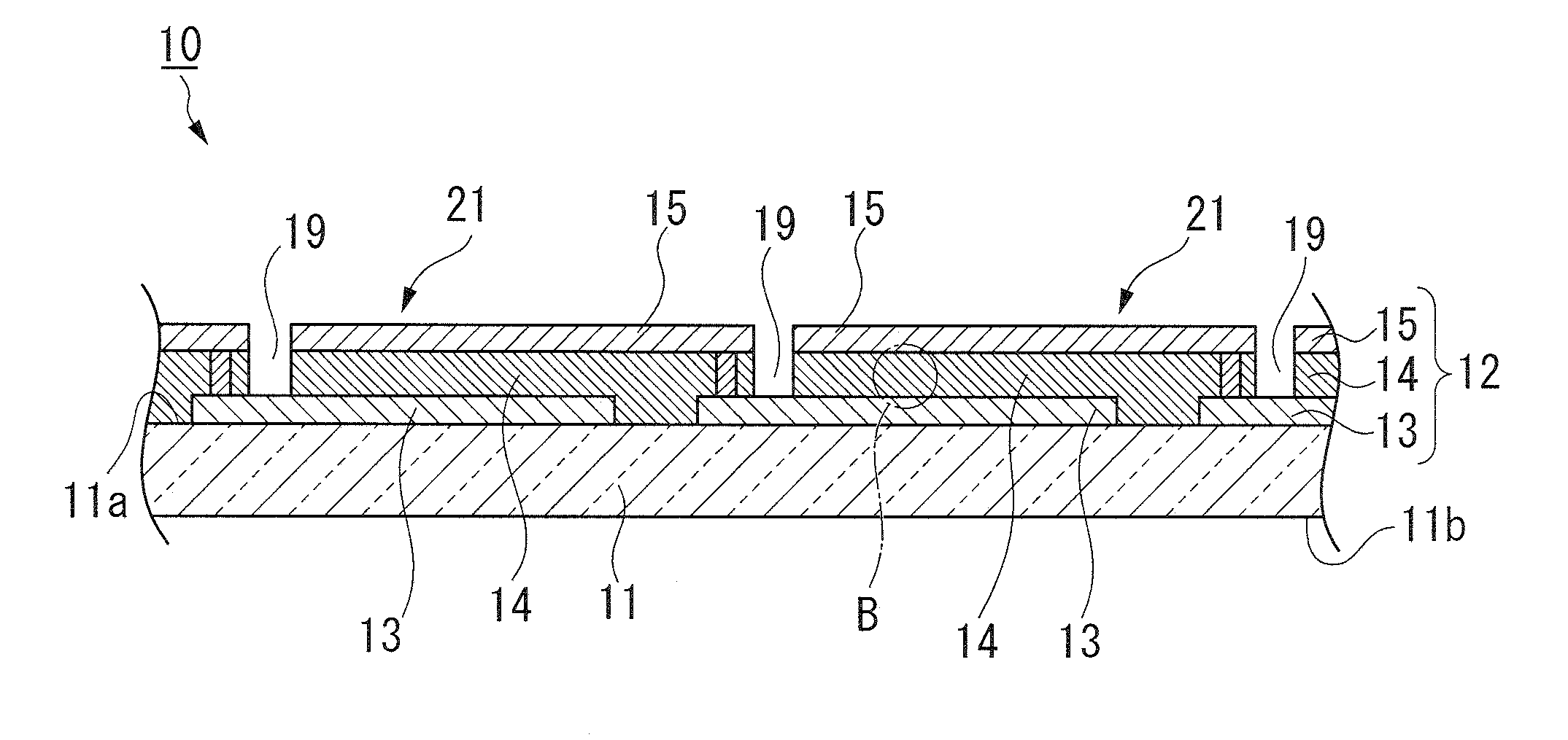
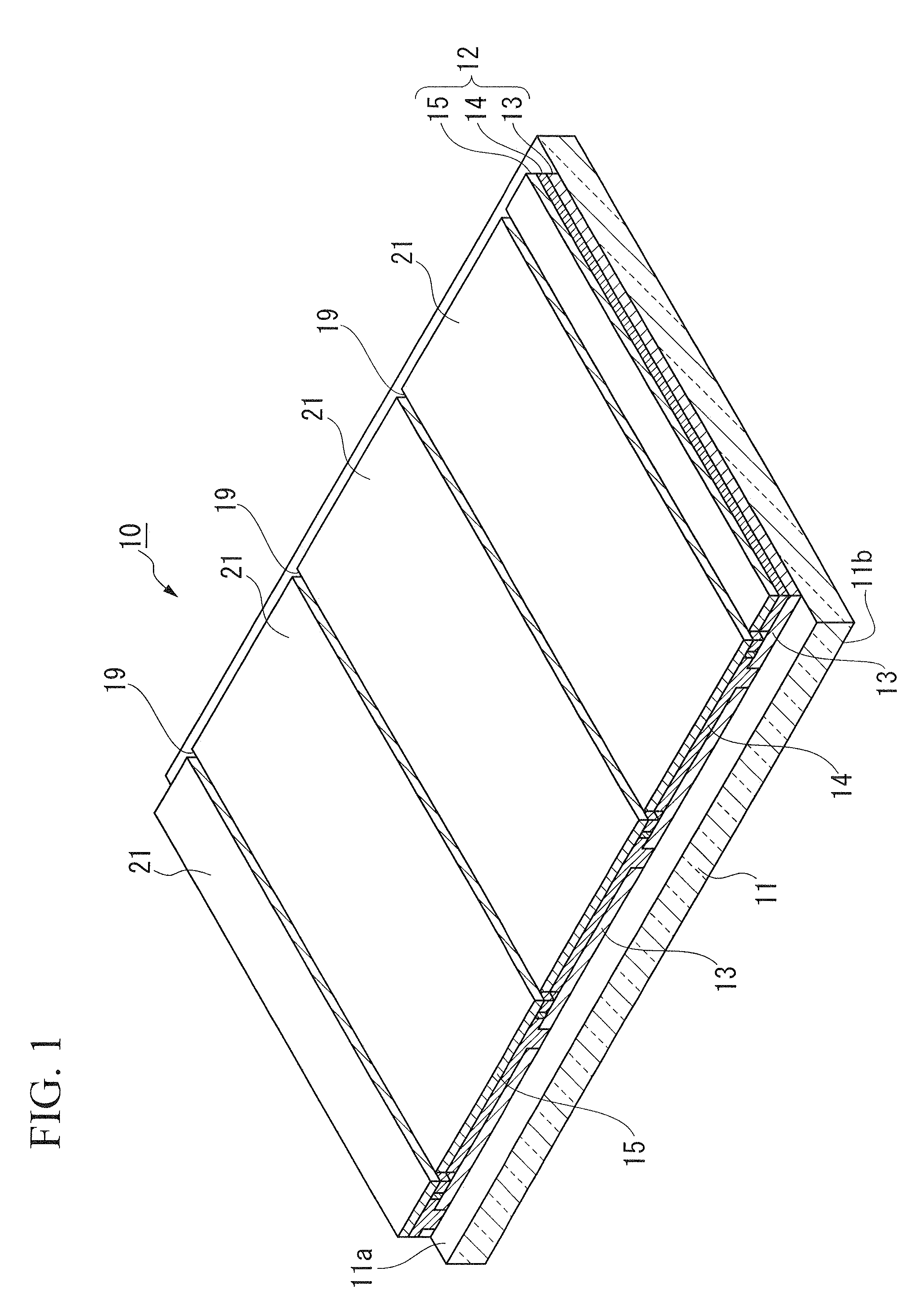
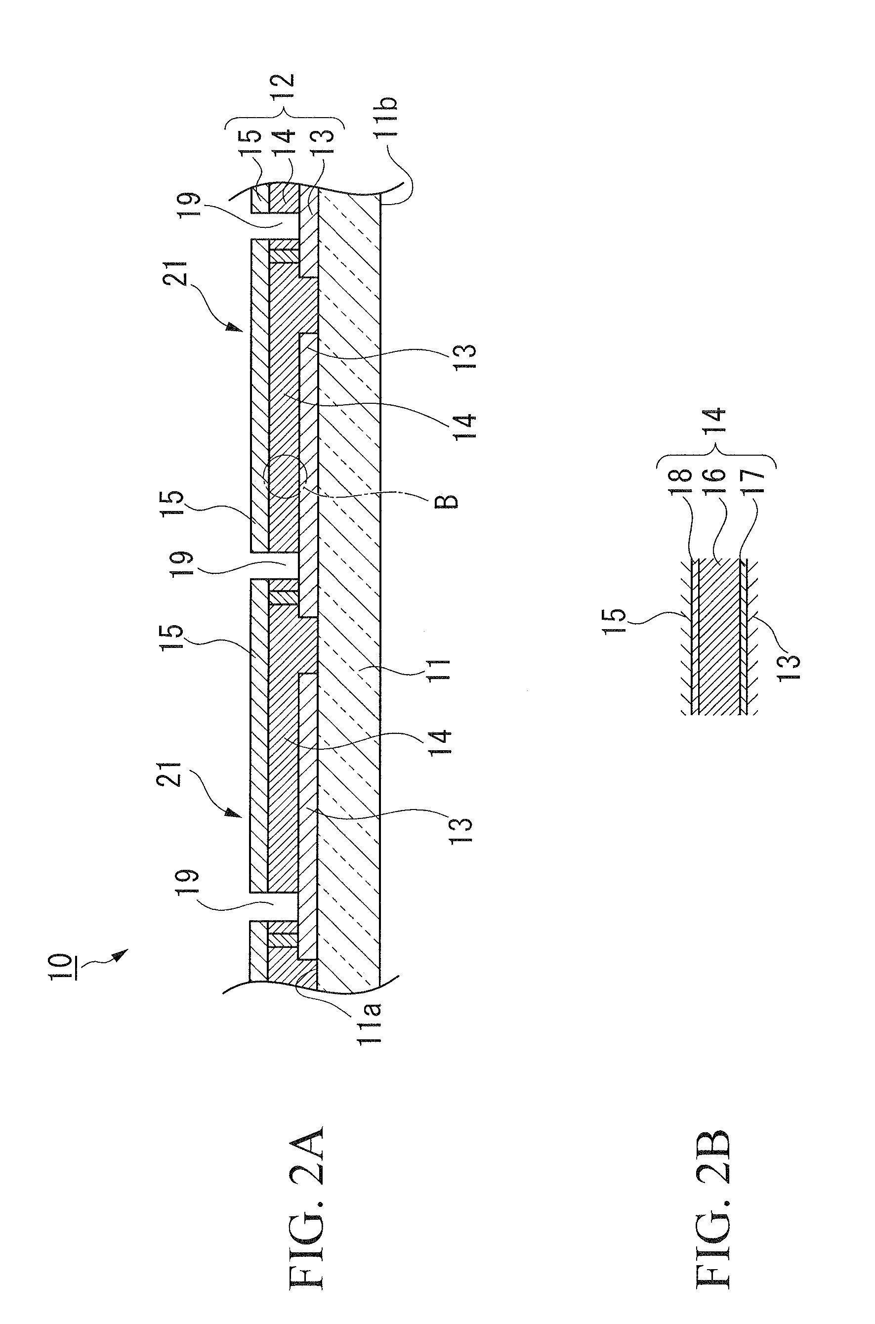
A photovoltaic cell manufacturing method includes: forming a photoelectric converter which has a plurality of compartment elements that are separated by a scribing line and in which adjacent compartment elements are electrically connected; detecting a structural defect existing in the compartment element; specifying a position in which the structural defect exists, as distance data indicating a distance between the structural defect and the scribing line that is closest to the structural defect; and removing a region in which the structural defect exists based on the distance data.

Description

BACKGROUND OF THE INVENTION[0001]1. Field of the Invention[0002]The present invention relates to a photovoltaic cell manufacturing method and a photovoltaic cell manufacturing apparatus, particularly, a photovoltaic cell manufacturing method and a photovoltaic cell manufacturing apparatus in which it is possible to quickly detect and repair a structural defect at a low cost.[0003]This application claims priority from Japanese Patent Application No. 2008-283166 filed on Nov. 4, 2008, the contents of which are incorporated herein by reference in their entirety.[0004]2. Background Art[0005]In recent years, in view of efficient use of energy, photovoltaic cells have been more widely used than ever before.[0006]Specifically, a photovoltaic cell in which a silicon single crystal is utilized has a high level of energy conversion efficiency per unit area.[0007]However, in contrast, in the photovoltaic cell in which the silicon single crystal is utilized, a silicon single crystal ingot is sl...

Claims


Application Information

Patent Timeline
IPC IPC(8): H01L31/18B23K26/02
CPCH01L31/208Y02E10/50Y10T29/53087Y10T29/53022H01L31/046Y02P70/50H01L31/04H01L31/18
Inventor YAMAMURO, KAZUHIROYUYAMA, JUNPEIYAMANE, KATSUMI
Owner ULVAC INC
Learn More