Connector And Semiconductor Testing Device Having The Same

Active Publication Date: 2011-11-17
MOLEX JAPAN +1
View PDF5 Cites 6 Cited by
  • Summary
  • Abstract
  • Description
  • Claims
  • Application Information

AI Technical Summary

Benefits of technology

[0007]The Present Disclosure is the result of contemplation on the problem described above. Accordingly, the object thereof is to provide a contact, and a semiconductor testing device utilizing such a contact. Consequently, the Present Disclosure presents a device able to suppress impedance mismatch and crosstalk, wherein terminals can be designed easily so as to not have a tendency for interferences between the contacting portions.
[0015]Further, in the semiconductor testing device according to the Present Disclosure, the signal terminal may have, at the lower end thereof, a contacting portion for contacting the circuit board, and each individual ground terminal may have two inner contacting portions and two outer contacting portions. Furthermore, a conductive pattern for contacting the contacting portion of the signal terminal, and a conductive pattern for contacting the two outer contacting portions and the two inner contacting portions, formed encompassing the signal conductive pattern, may be formed on the surface of the circuit board. Thus, the contacting portion of the signal terminal can be encompassed by the two inner contacting portions and the two outer contacting portions, enabling suppression of the impedance mismatch and the crosstalk. Additionally, the conductive pattern that contacts the inner contacting portions and the outer contacting portions (that is, the ground conductive pattern) encompasses the conductive pattern that contacts the contacting portion for the signal terminal (that is, the signal propagation conductive pattern), and thus it is possible to achieve excellent impedance matching even on the circuit board. Note that the number of inner contacting portions or outer contacting portions is not limited to two.

Problems solved by technology

Accordingly, there is a tendency for impedance mismatch and crosstalk to occur in the vicinity of the contacting portions.
However, when the number of contacting portions is increased, there is a tendency to produce interferences between the contacting portions.
For example, in a structure wherein all of the contacting portions face toward the inside of a cylindrical ground terminal, there will be a tendency for there to be interferences between the contacting portions of the ground terminal, and for there to be interferences between the contacting portions of the ground terminal and the contacting portion of the signal terminal.
Moreover, in structures wherein all of the contacting portions face to the outside of the cylindrical ground terminal, there is a tendency for there to be interferences between the contacting portions of two grounds terminals that are adjacent to each other.

Method used


Image

  • Connector And Semiconductor Testing Device Having The Same
  • Connector And Semiconductor Testing Device Having The Same
  • Connector And Semiconductor Testing Device Having The Same

Examples


Embodiment Construction

[0027]While the Present Disclosure may be susceptible to embodiment in different forms, there is shown in the Figures, and will be described herein in detail, specific embodiments, with the understanding that the disclosure is to be considered an exemplification of the principles of the Present Disclosure, and is not intended to limit the Present Disclosure to that as illustrated.

[0028]In the embodiments illustrated in the Figures, representations of directions such as up, down, left, right, front and rear, used for explaining the structure and movement of the various elements of the Present Disclosure, are not absolute, but relative. These representations are appropriate when the elements are in the position shown in the Figures. If the description of the position of the elements changes, however, these representations are to be changed accordingly.

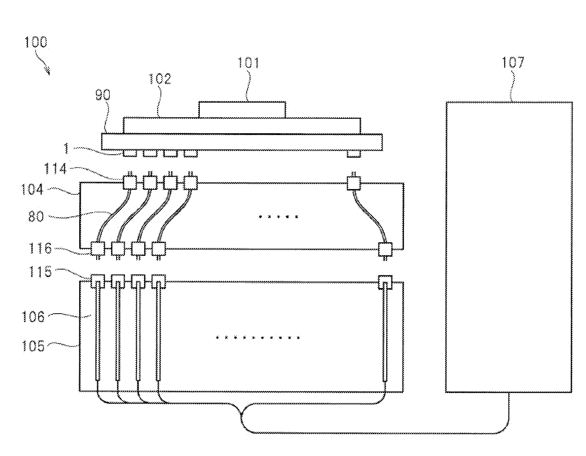
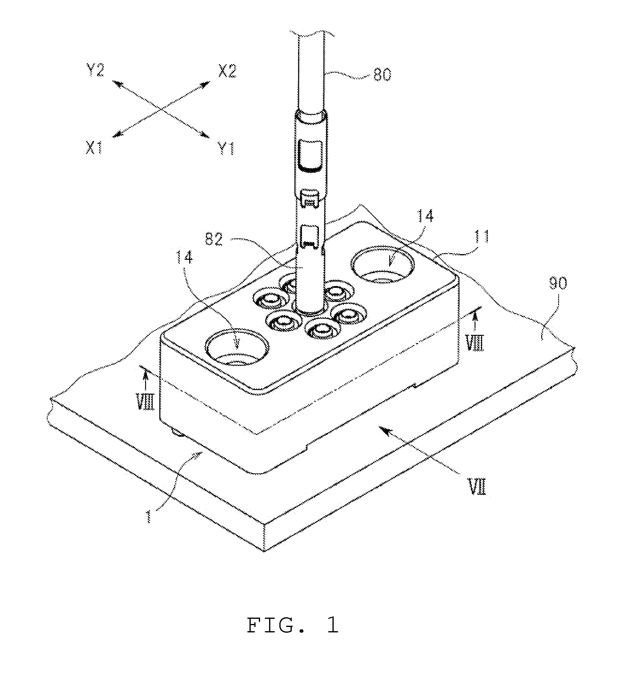
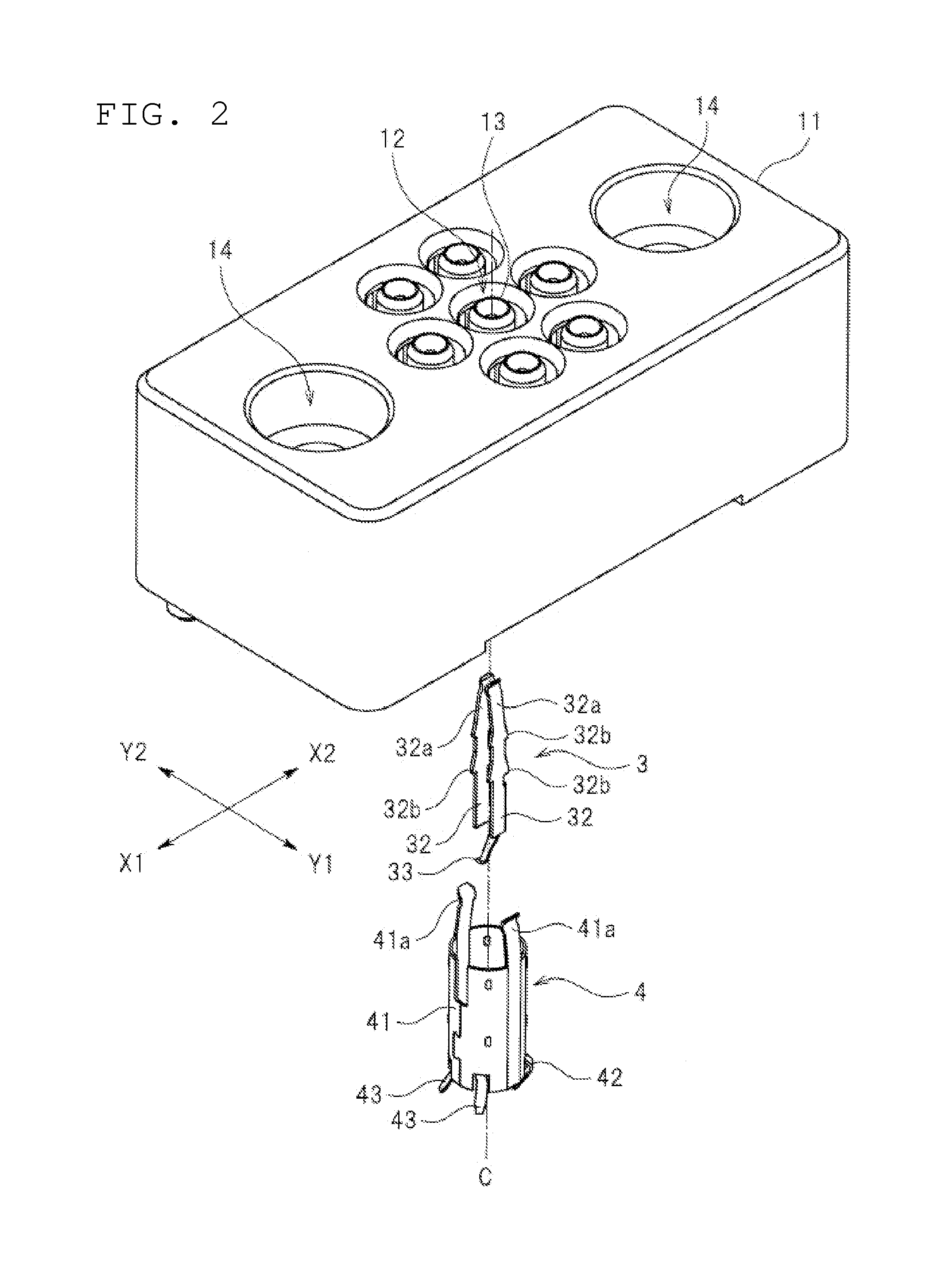
[0029]Further, note that in the Present Disclosure, the perpendicular direction relative to the circuit board 90 to which the connector...


PUM


Abstract

To provide a connector wherein ground terminals can be designed easily, which not only suppresses the occurrence of impedance mismatch and crosstalk, but which does not lead to interferences between contacting portions. A ground terminal for a connector has a cylindrical main body. A plurality of contacting portions, for contacting a circuit board, are formed on the bottom edge of the cylindrical main body. The ground terminal has, as contacting portions, inner contacting portions and outer contacting portions. The inner contacting portions extend toward the inside of the cylindrical main body and in the downward direction, and the outer contacting portions extend toward the inside of the cylindrical main body and in the downward direction.

Description

CROSS REFERENCE TO RELATED APPLICATIONS[0001]The Present Disclosure claims priority to prior-filed Japanese Patent Application No. 2010-109655, entitled “Connector And Semiconductor Testing Device Having The Same,” filed on 11 May 2010 with the Japanese Patent Office. The content of the aforementioned Patent Application is fully incorporated in its entirety herein.BACKGROUND OF THE PRESENT DISCLOSURE[0002]The Present Disclosure relates, generally, to a connector that can connect to a coaxial cable, and to a semiconductor testing device having such a connector, and, further, to technology for suppressing crosstalk and impedance mismatch.[0003]Conventionally, connectors have been used for connecting coaxial cables to circuit boards. Such connectors typically have a plurality of ground terminals that make contact with shield lines in coaxial cables, and a plurality of signal terminals that make contact with signal lines of coaxial cables. Moreover, in such connectors, individual termin...

Claims


Application Information

Patent Timeline
IPC IPC(8): G01R31/00H01R12/71
CPCG01R1/0416H01R24/50H01R12/714G01R31/2822G01R31/26H01R13/646
Inventor UESAKA, RYOWATANABE, JUNMIZUMURA, AKINORIWAGATA, HIROTAKA
Owner MOLEX JAPAN
Why Eureka
Try Eureka