
Novel Compound, Method of Producing the Compound, Organic Semiconductor Material and Organic Semiconductor Device

Inactive Publication Date: 2011-09-15
HIROSHIMA UNIVERSITY
View PDF3 Cites 15 Cited by
  • Summary
  • Abstract
  • Description
  • Claims
  • Application Information

AI Technical Summary

Benefits of technology

[0026]The compound of the present invention has a naphthalene-thiophene skeleton or a naphthalene-selenophene skeleton. The compound has a conjugate system in each molecule due to an interaction between π orbitals, and shows a strong molecular interaction through a sulfur atom or a selenium atom contained in a thiophene ring or a selenophene ring in each molecule. Hence, carriers can move efficiently. Because the compound of the present invention has good field mobility, such a compound can be used as an organic semiconductor material. This organic semiconductor material can be used for an organic semiconductor device.
[0027]Moreover, according to the production method of the compound of the present invention, it becomes possible to produce a compound having a naphthalene-thiophene skeleton or a naphthalene-selenophene skeleton through the form of a dihalogeno-diethynylnaphthalene derivative.
[0028]Furthermore, according to the production method of the compound of the present invention, it becomes possible to cause a hydrogen atom of naphthalene to be selectively subjected to halogenation. According to this method, the yield of the compound having a naphthalene-thiophene skeleton or a naphthalene-selenophene skeleton can be improved.

Problems solved by technology

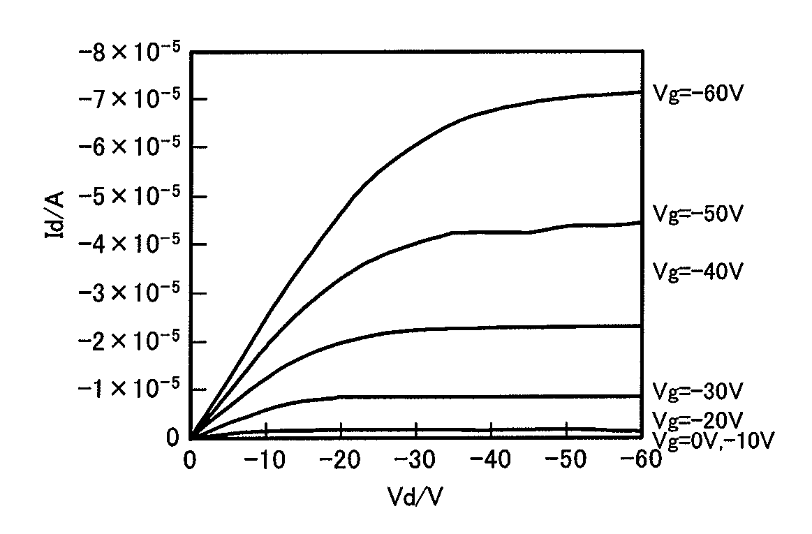
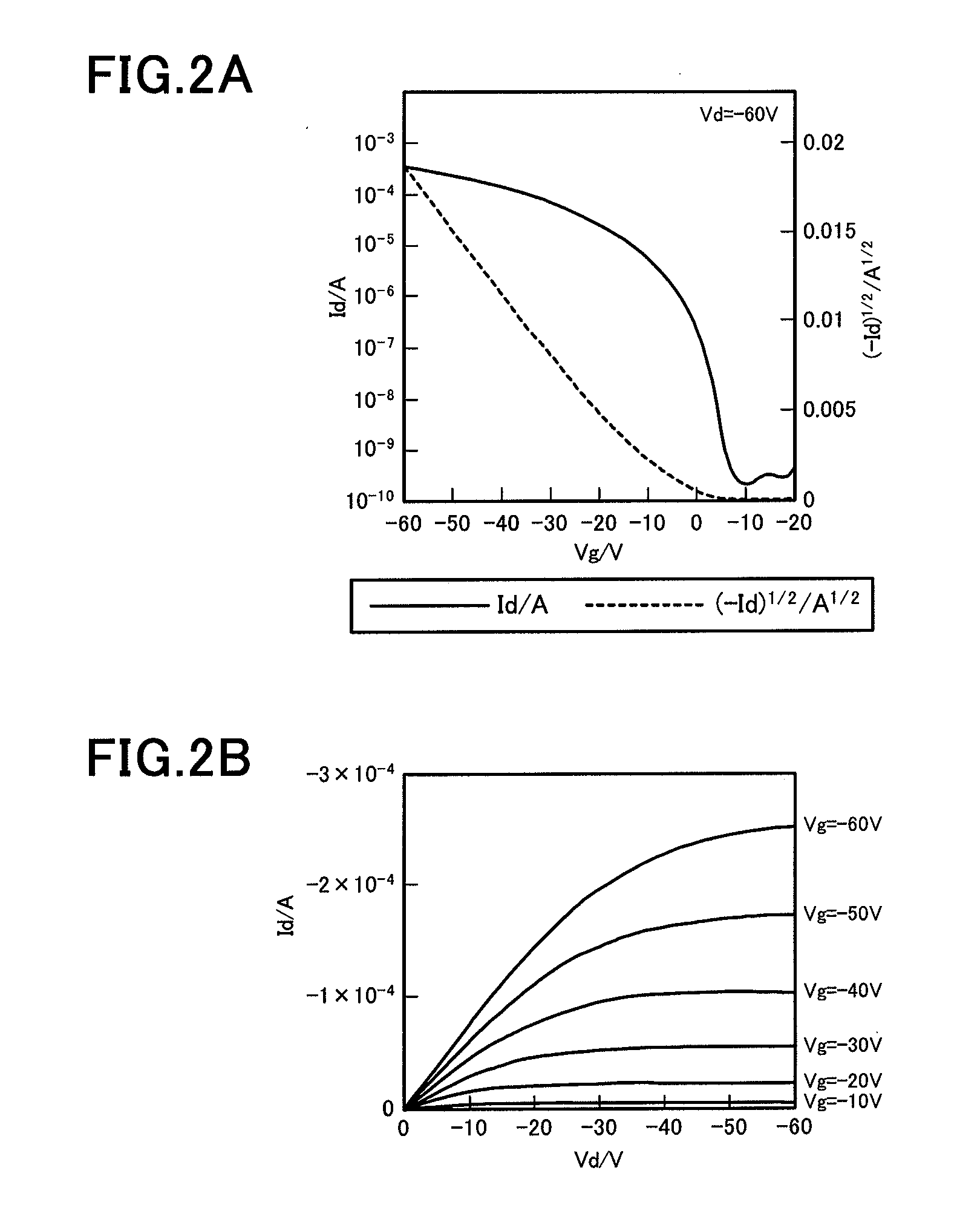
Moreover, in the case of an organic FET device, the mobility of carrier directly affects the switching speed of a transistor and the performance of a device to be driven.

Method used


Image

  • Novel Compound, Method of Producing the Compound, Organic Semiconductor Material and Organic Semiconductor Device
  • Novel Compound, Method of Producing the Compound, Organic Semiconductor Material and Organic Semiconductor Device
  • Novel Compound, Method of Producing the Compound, Organic Semiconductor Material and Organic Semiconductor Device

Examples


examples

[0093]The compound of the present invention and the production method thereof will be explained through specific examples below.

first example

[0094]An explanation will be given of synthesis of the compound represented by the general formula (1) and having the liner structure. Note that the structure of the compound is set through 1H NMR (1H Nuclear Magnetic Resonance spectrum) and EIMS (mass spectrography spectrum). The apparatuses used for measurement of respective spectra are as follows:

[0095]1H-NMR: JEOL Lambda 400 spectrometer[0096]: JEOL EX-270 spectrometer

[0097]EIMS: Shimadzu QP-5050A

[0098]Those apparatuses were also used in other examples to be discussed later.

[0099]An explanation will be given of synthesis of naphtho[2,3-b:6,7-b′]dithiophene step by step.

Synthesis of 1,3,5,7-tetrabromo-2,6-dihydroxynaphthalene

[0100]2,6-dihydroxynaphthalene (2 g, 12.5 mol) was dissolved in acetic acid (60 ml). The acetic acid was used as a solvent. Bromine (2.6 ml. 50.7 mol) was dripped in the solution, and reaction was carried out under a reflux temperature (120° C. to 125° C.).

[0101]As is explained in the embodiment for carrying ...

second example

[0135]Next, an explanation will be given of synthesis of 2,7-diphenylnaphto[2,3-b:6,7-b′]dithiophene step by step.

Synthesis of 2,6-dibromo-3,7-bis(phenylethynyl)naphthalene

[0136]Using 3,7-dibromo-2,6-bis(trifluoromethanesulfonyl)naphthalene synthesized through the above-explained method, 2,6-dibromo-3,7-bis(phenylethynyl)naphthalene was synthesized through the following procedures.

[0137]Under a nitrogen atmosphere, 3,7-dibromo-2,6-bis(trifluoromethanesulfonyl)naphthalene (582 mg, 1.0 mmol) was dissolved in DMF (7 ml) and diisopropylamine (7 ml). The solution was degassed for 30 minutes.

[0138]Pd(PPh3)2Cl2 (70 mg, 0.05 mmol, 10 mol %) and CuI (38 mg, 0.1 mmol, 20 mol %) as catalysts, and phenylacetylene (0.22 ml, 2.0 mmol) as a reagent were added to the solution, and the solution was stirred for 11 hours at a room temperature in order to let it reacted. Thereafter, pure water (1 ml) and 1N hydrochloric acid (1 ml) were added in order to terminate the reaction.

[0139]The reaction soluti...


PUM


Abstract

There are provided a novel compound having a good field mobility, a method of producing of the compound, an organic semiconductor material containing the novel compound, and an organic semiconductor device. The novel compound which is represented by the following general formula (1), (2), (3) or (4) (where Z represents a sulfur atom or a selenium atom, and R represents a hydrogen atom, an alkyl group or a phenyl group in general formulae) has a structure having two benzene rings of naphthalene bonded with a thiophene ring and a selenophene ring, respectively. These compounds have a conjugate system in molecules due to an interaction between it orbitals, and show a strong molecular interaction through a sulfur atom or a selenium atom contained in a thiophene ring or a selenophene ring in each molecule, thereby having a good field mobility.

Description

CROSS REFERENCES TO RELATED APPLICATION[0001]This application is a US National Phase application of International Patent Application No. PCT / JP2009 / 068660 filed 30 Oct. 2009, and claims priority to Japanese Patent Application No. 2008-298830 filed on 21 Nov. 2008 and Japanese Patent Application No. 2009-080527 filed 27 Mar. 2009. The disclosures of the above Japanese Patent Applications are incorporated herein by reference in its entirety.TECHNICAL FIELD[0002]The present invention relates to a novel compound, a method of producing the compound, an organic semiconductor material and an organic semiconductor device.BACKGROUND ART[0003]Recently, thin-film devices using organic semiconductor materials, such as organic EL (Electro Luminescence) devices, organic FET (Field Effect Transistor) devices, and organic thin-film photoelectric conversion devices, are getting attention, and become in a practical use.[0004]The mobility of electronic charge carrier (hereinafter, simply referred to a...

Claims


Application Information

Patent Timeline
IPC IPC(8): C07D495/02C07D517/02
CPCC07D495/04C07D517/04H01L51/0545H01L51/0074H01L51/0541H01L51/0071H10K85/6576H10K85/657H10K10/464H10K10/466H10K10/00
Inventor TAKIMIYA, KAZUO
Owner HIROSHIMA UNIVERSITY
Learn More