
Micro-composite pattern lens, and method for manufacturing same

Inactive Publication Date: 2011-09-01
BLUEN
View PDF2 Cites 18 Cited by
  • Summary
  • Abstract
  • Description
  • Claims
  • Application Information

AI Technical Summary

Benefits of technology

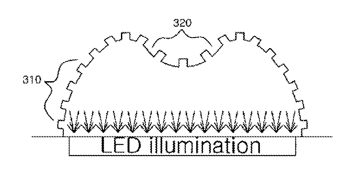
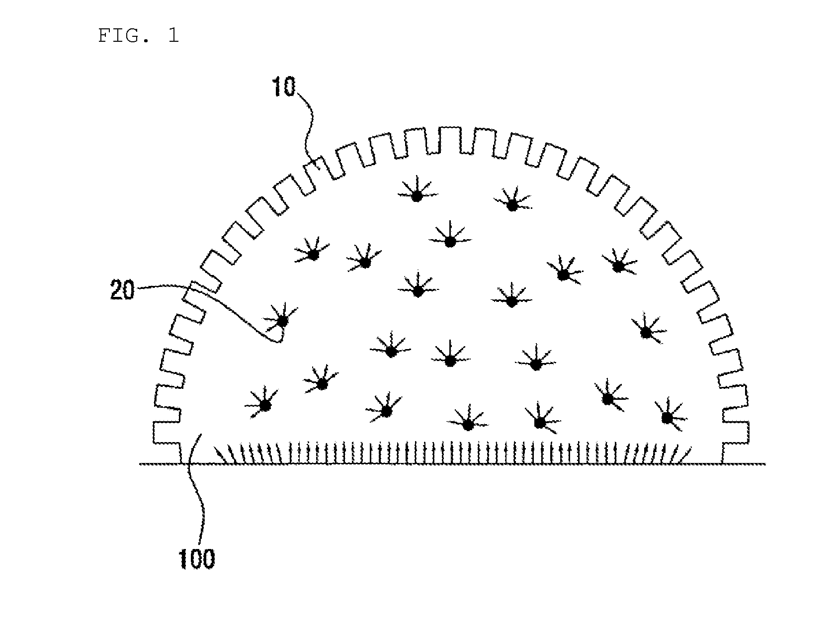
[0006]To achieve the object of the present invention, Further, the micro-composite pattern lens according to the present invention can form a wider angle of light emission, thus enabling an LED source, which is a point light source, to be converted into a surface light source having superior luminous intensity uniformity. Further, the lens of the present invention is advantageous in that a single lens may serve as a light guide plate, a prism plate, and a diffusion plate, thus eliminating the necessity of stacking optical plates, which might otherwise be required for conventional backlight units. Further, according to the present invention, the angle of light emission of the LED source which is approximately 90 degrees can be widened to 160 degrees or higher, and the local change in the micro-pattern and the mixture of ultrafine particles may improve the luminous intensity uniformity and the angle of emission of the light source. Also, wafer levels can be manufacture using a microfluidic channel array based on three dimensional molding techniques and the mixture of ultrafine particles. In addition, the use of single lens having a wider angle of light emission reduces the number of LEDs, thus reducing manufacturing costs and heat generated by LEDs. Further, the micro-composite pattern lens of the present invention has a double curvature structure to achieve improved luminous intensity uniformity and an improved angle of light emissions as compared to a single curvature structure.

Problems solved by technology

However, since domestic LED enterprises import the LED lens from Europe or Japan or provide the lens in a manner of joint development with foreign enterprises, domestic lens development is an urgent problem.
Since brightness depends on lens of LEDs, the technical importance thereof is very large.
Further, the lens occupy the weight of 5% or less in total LED production cost, but it is expected that the cost is higher in a case of high output LED.
Even though a prior lens provided over LED has possibly improved the angle of light emission, there are problems of limiting to control the luminous intensity uniformity and requiring various composite optical plates such as a light guide plate, a prism plate, a diffusion plate when converting a point light source such as LED into a surface light source.
Since the production process cost for each element is higher and accurate packaging is required, there is a limitation to reduce overall production cost and so integrated optical element is requested.

Method used


Image

  • Micro-composite pattern lens, and method for manufacturing same
  • Micro-composite pattern lens, and method for manufacturing same
  • Micro-composite pattern lens, and method for manufacturing same

Examples


production example

[0101]FIG. 16 is a process diagram illustrating a method of manufacturing the micro-composite pattern lens having double curvature structure according to one embodiment of the present invention.

[0102]Referring to (a) of FIG. 16, a photo-resist was stacked on a substrate and then patterned to make the micro pattern array 2. According to one embodiment of the present invention, the silicone substrate of 4 inches was washed and then water remaining over it was evaporated at a temperature of 120° C. for 30 seconds. As a result, chemical residue and organic contaminants were moved. Further, a bonding force between the photo-resist and the silicone substrate is improved due to HMDS treatment. Then, AZ1512 (AZ Electronic Materials) which is a positive photo-resist was applied to the silicone substrate and then spin-coated at 1500 rmp for 3 seconds and 450 rmp for 30 seconds, which results that the photo-resist layer of 1.2 μm is stacked on the silicone substrate. Subsequently, the positive...

experimental example

[0113]A relationship between the curvature structure of the lens and the angle of light emission was analyzed via this experimental example. The angle of the emission light of the micro-composite pattern lens having double curvature structure was measured and analyzed using optical power meter. The LED light source was used as a reference example, and micro-composite pattern lens of concave lens and convex lens having a single curvature structure was used as comparison example.

[0114]FIG. 18 is a graph measuring an angle of light emission of the LED light source.

[0115]Referring to FIG. 18, it will be appreciated that the micro-composite pattern lens having double curvature structure according to the present invention has a wider angle of light emission than the micro-composite pattern lens having single curvature structure.

[0116]The experiment result represents that the angle of light emission depends on the curvature structure of the lens and particularly the double structure is adv...


PUM

PropertyMeasurementUnit
Angleaaaaaaaaaa
Angleaaaaaaaaaa
Thicknessaaaaaaaaaa

Abstract

The present invention relates to a micro-composite pattern lens and to a method for manufacturing same. The micro-composite pattern lens of the present invention has a micro-composite pattern with one or more protrusions formed on one side of the lens having a predetermined curvature, and optical polymer nanoparticles arranged in the lens. The micro-composite pattern of the lens may form a wider angle of light emission, thus enabling an LED source, which is a point light source, to be converted into a surface light source having superior luminous intensity uniformity. The lens of the present invention is advantageous in that a single lens may serve as a light guide plate, a prism plate, and a diffusion plate, this eliminating the necessity of stacking optical plates, which might otherwise be required for conventional backlight units. According to the present invention, the angle of emission of the LED source which is approximately 90 degrees can be widened to 160 degrees or higher, and the local change in the micro-pattern and the mixture of ultrafine particles may improve the luminous intensity uniformity and the angle of emission of the light source. Also, wafer levels can be manufactured using a microfluidic channel array based on three dimensional molding techniques and the mixture of ultrafine particles. In addition, the use of single lens having a wider angle of light emission reduces the number of LEDs, thus reducing manufacturing costs and heat generated by LEDs. Further, the micro-composite pattern lens of the present invention has a double curvature structure to achieve improved luminous intensity uniformity and an improved angle of light emission as compared to a single curvature structure.

Description

TECHNICAL FIELD[0001]The present invention relates to micro-composite pattern lens; and, more particularly, to micro-composite pattern lens and a method for manufacturing the same which causes the light emitted from the light source to have a wider angle of light emission and superior luminous intensity uniformity.BACKGROUND ART[0002]At present, various technologies have been developed to control the light by deforming a surface of the lens using elaborate Micro Electro Mechanical System (MEMS) process. Among them, a research for distributing the light in a wide and uniform manner has been drawn a great attention.[0003]Particularly, since there are known many advantages in LEDs (Light Emitting Diodes) backlight units (hereinafter, referred to BLUs) rather than BLUs used in existing LCD-TV, the LED BLUs have been commercially applied to TV.[0004]A function of the lens is gradually increasing since diffusivity is important in cases of LCD or LED light source for illuminating BLU. Howe...

Claims


Application Information

Patent Timeline
IPC IPC(8): H01L33/58G02B13/14B29C33/42G02B1/12B82Y40/00
CPCB29D11/00009B29D11/00326G02B5/02B82Y20/00G02B3/08B29D11/00346
Inventor JEONG, KI HUNCHAE, SUN KIJUNG, HYUK JINKIM, JAE JUN
Owner BLUEN
Learn More