Image sensor with improved black level calibration
a technology of image sensor and black level, applied in the field of image sensors, can solve the problems of degrading the picture provided by the imaging system, generating inaccurate image data for image sensors, and affecting the image quality of the image sensor
- Summary
- Abstract
- Description
- Claims
- Application Information
AI Technical Summary
Benefits of technology
Problems solved by technology
Method used
Image
Examples
first embodiment
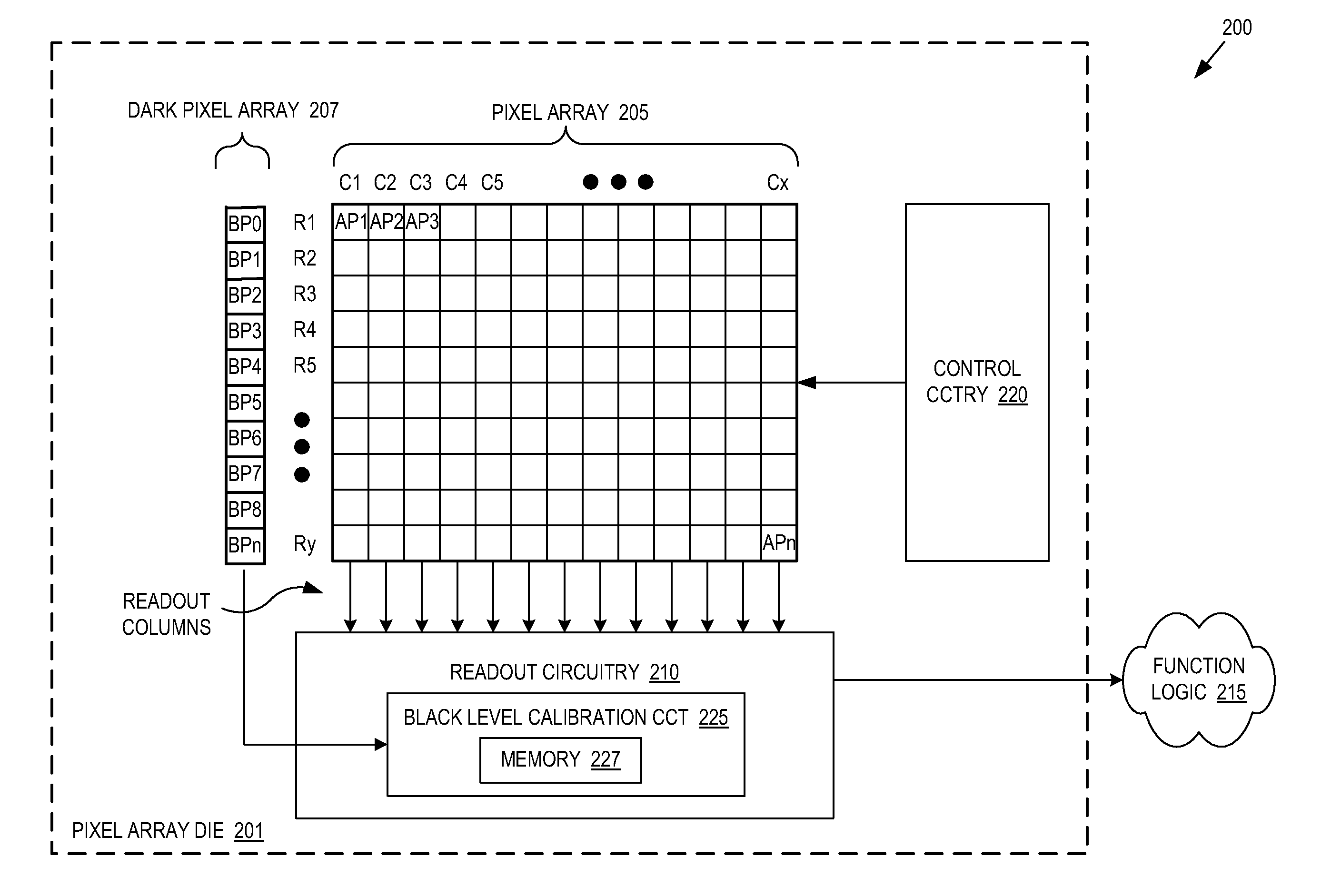
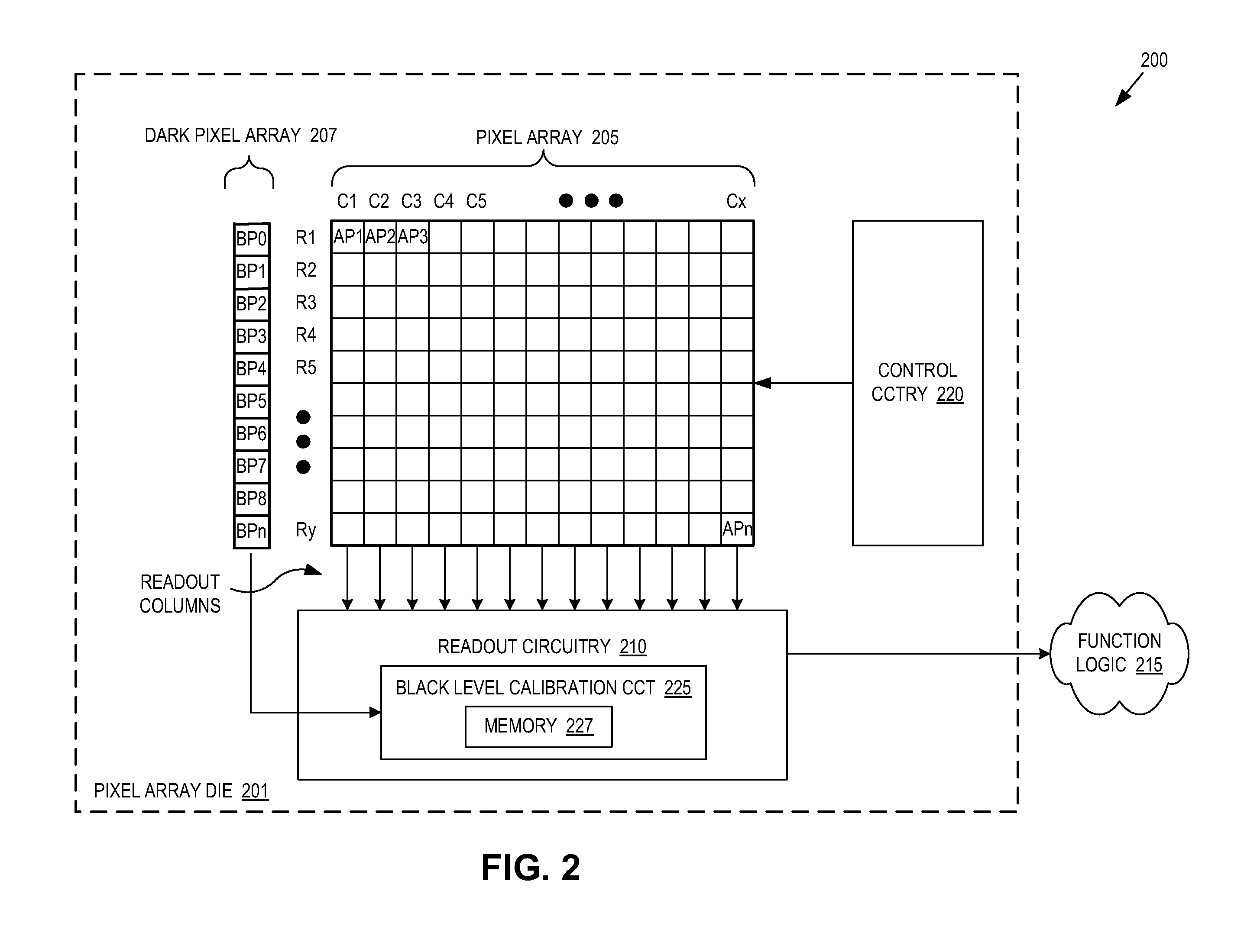
[0041]FIG. 6 is a cross-sectional view of a BSI image sensor 600 illustrating an imaging pixel array, a dark pixel array, and peripheral circuitry (i.e., circuitry that is peripheral to the imaging pixel array) in relation to a light blocking layer, in accordance with a FIG. 6 shows light shielding layer 590 and buffer layer 579 disposed in the light path to dark pixel array 207 and under the readout and control circuitry 201, 220. FIG. 6 further illustrates how antireflective layers 576 and 577 rejoin in the light path to pixel array 205 to provide the equivalent function of antireflective layer 478 of active pixel 400 as shown in FIG. 4. A planarizing layer 605 is formed in the light path of pixel array 205 in order to provide a planar surface for the formation of color filter 410 and microlenses 415. Planarizing layer 605 compensates for the added thicknesses of layers 590 and 579. In one embodiment, planarizing layer 605 is formed of a polymer material.
[0042]It was observed tha...
second embodiment
[0043]FIG. 7 is a cross-sectional view of a BSI image sensor 700 illustrating imaging pixel array 205, dark pixel array 207, and peripheral circuitry (e.g., readout circuitry 210 and control circuit 220) in relation to a light shielding layer 790, in accordance with a FIG. 7 illustrates how buffer layer 779 does not extend under dark pixel array 207, but is retained under the peripheral circuitry and continues to act as an etch stop in the areas where light shielding layer 790 is patterned and removed.
third embodiment
[0044]FIG. 8 is a cross-sectional view of a BSI image sensor illustrating imaging pixel array 205, dark pixel array 207, and peripheral circuitry in relation to light shielding layer 790, in accordance with a FIG. 8 illustrates how a portion of buffer layer 779 has been removed under dark pixel array 207, but retained elsewhere and continues to act as an etch stop in the areas where light shielding layer 790 is removed. The illustrated embodiment of FIG. 8 further includes a stress adjusting layer 892 disposed above light shielding layer 790 and under buffer layer 779 and antireflective layer 576. Stress adjusting layer 892 is deposited after removal of selected portions of buffer layer 779 and lies above those portions of light shielding layer 790 that remain after its photolithographic patterning. In one embodiment, light shielding layer 790 is formed of silicon oxide or silicon nitride. During fabrication, the properties of these layers can be controlled such that the stress imp...
PUM
 Abstract
Description
Claims
Application Information
 - R&D
- Intellectual Property
- Life Sciences
- Materials
- Tech Scout
- Unparalleled Data Quality
- Higher Quality Content
- 60% Fewer Hallucinations
Browse by: Latest US Patents, China's latest patents, Technical Efficacy Thesaurus, Application Domain, Technology Topic, Popular Technical Reports.
© 2025 PatSnap. All rights reserved.Legal|Privacy policy|Modern Slavery Act Transparency Statement|Sitemap|About US| Contact US: help@patsnap.com


