
High-Throughput Combinatorial Dip-Coating Apparatus and Methodologies

a dip coating and high-throughput technology, applied in the field of semiconductor and solar processing, can solve the problems of ever escalating r&d costs and the inability to conduct extensive experimentation in a timely and cost-effective manner

Inactive Publication Date: 2011-06-23
INTERMOLECULAR
View PDF12 Cites 2 Cited by
  • Summary
  • Abstract
  • Description
  • Claims
  • Application Information

AI Technical Summary

Problems solved by technology

This approach has resulted in ever escalating R&D costs and the inability to conduct extensive experimentation in a timely and cost effective manner.

Method used


Image

  • High-Throughput Combinatorial Dip-Coating Apparatus and Methodologies
  • High-Throughput Combinatorial Dip-Coating Apparatus and Methodologies
  • High-Throughput Combinatorial Dip-Coating Apparatus and Methodologies

Examples


Embodiment Construction

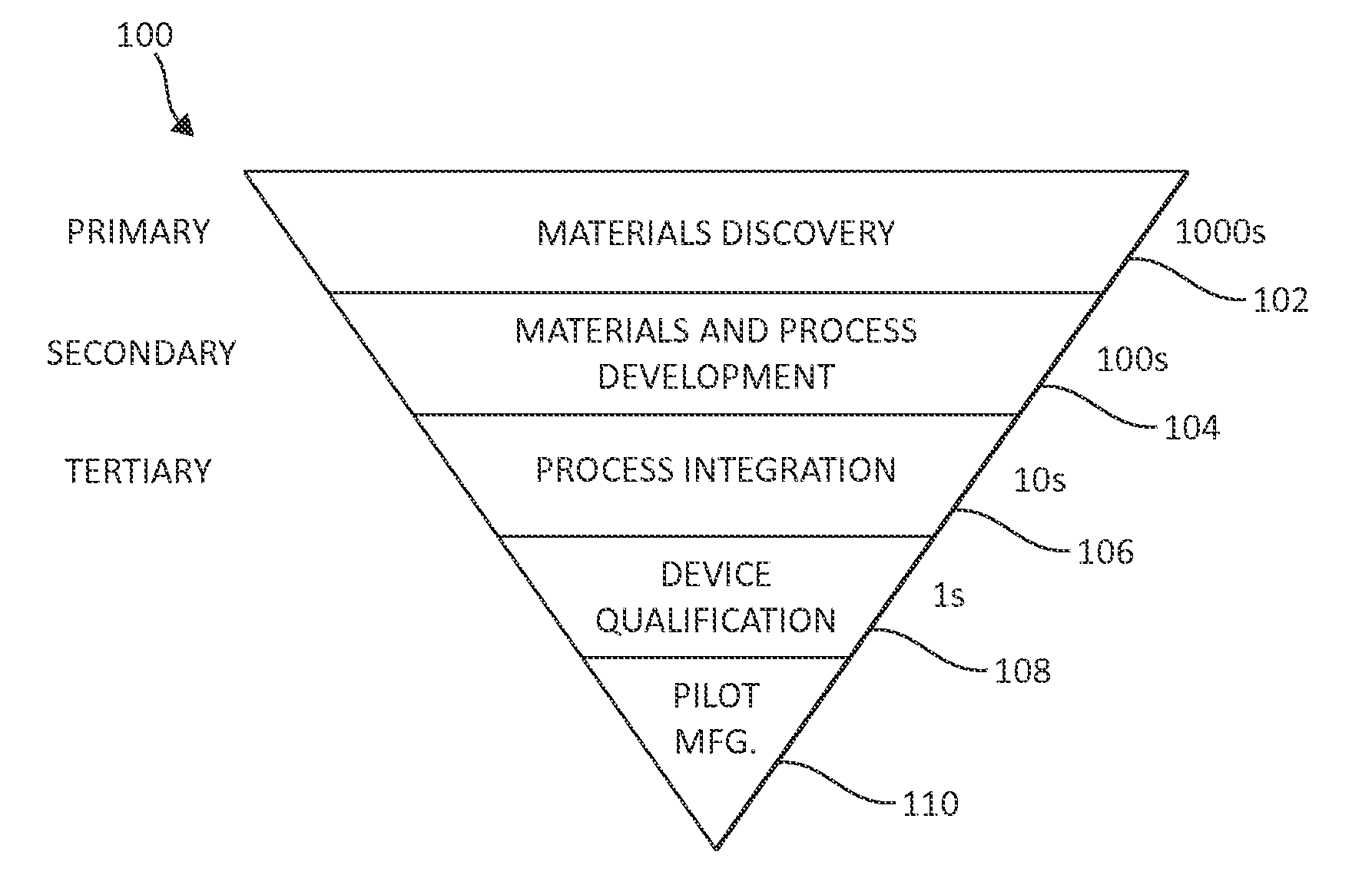
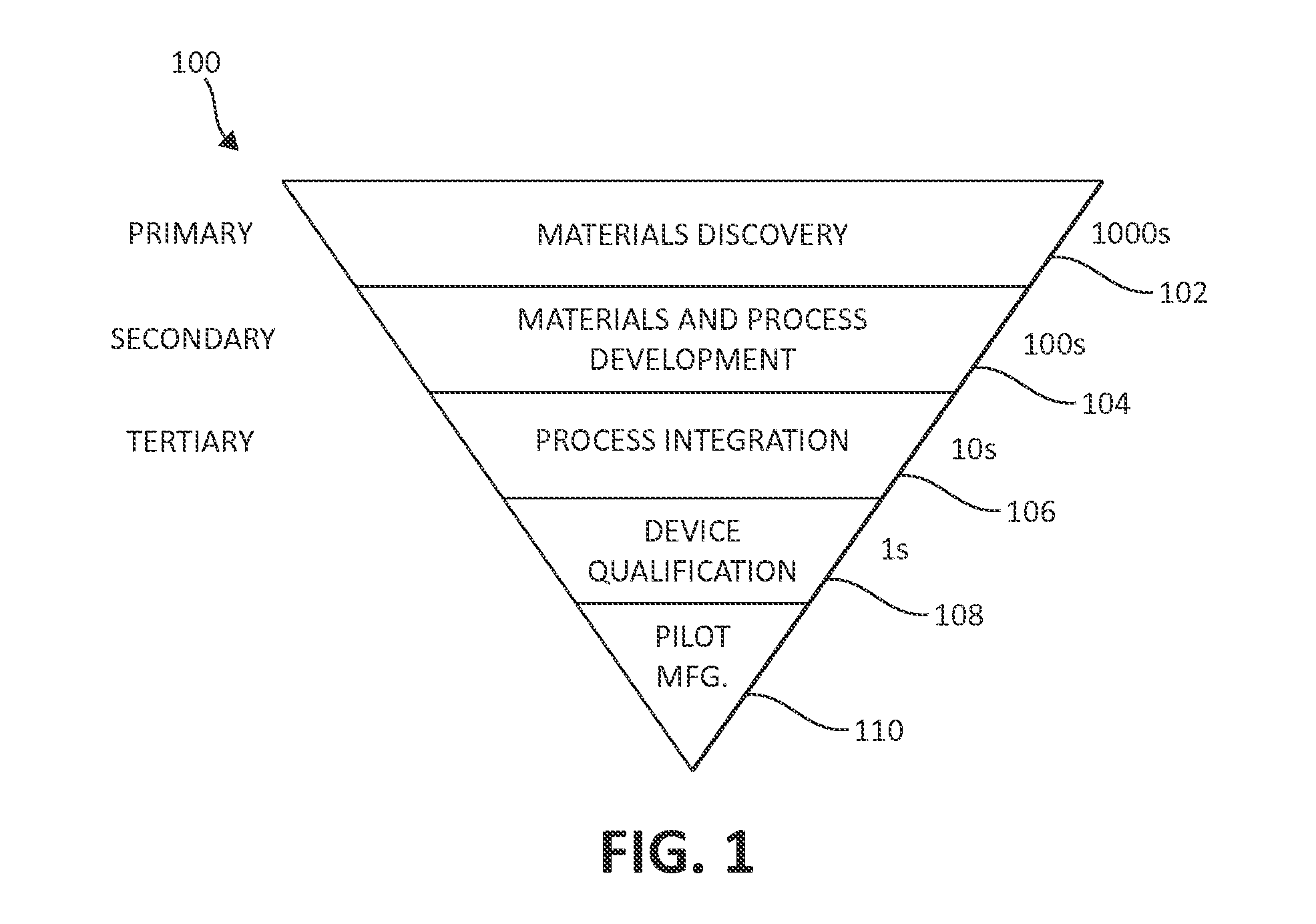
[0013]A detailed description of one or more embodiments is provided below along with accompanying figures. The detailed description is provided in connection with such embodiments, but is not limited to any particular example. The scope is limited only by the claims and numerous alternatives, modifications, and equivalents are encompassed. Numerous specific details are set forth in the following description in order to provide a thorough understanding. These details are provided for the purpose of example and the described techniques may be practiced according to the claims without some or all of these specific details. For the purpose of clarity, technical material that is known in the technical fields related to the embodiments has not been described in detail to avoid unnecessarily obscuring the description.

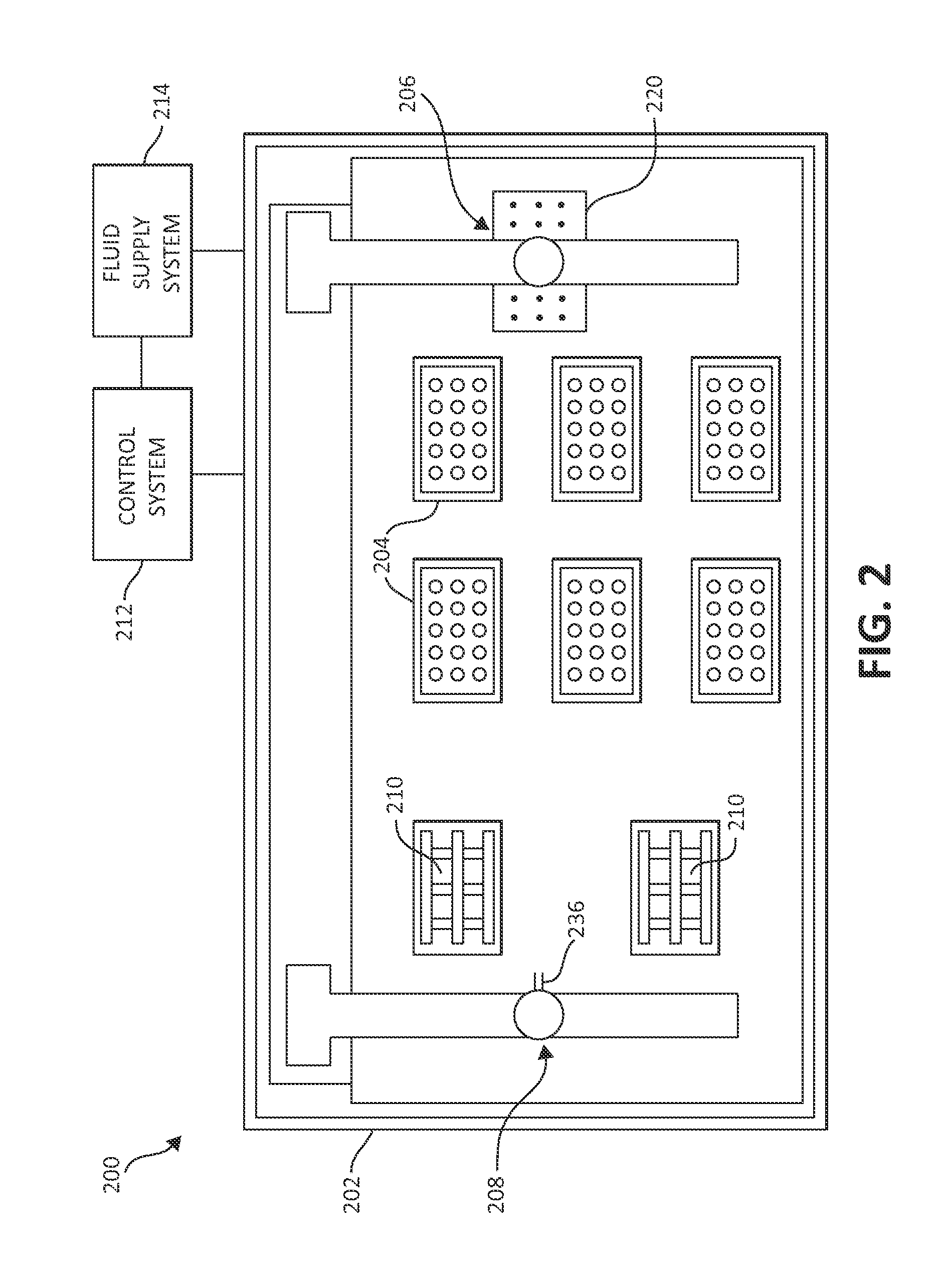
[0014]Embodiments of the current invention describe a high performance combinatorial apparatus for the combinatorial development of coatings by a dip-coating process. The dip-...


PUM

PropertyMeasurementUnit
Temperatureaaaaaaaaaa
Compositionaaaaaaaaaa

Abstract

Embodiments of the current invention describe a high performance combinatorial method and apparatus for the combinatorial development of coatings by a dip-coating process. The dip-coating process may be used for multiple applications, including forming coatings from varied sol-gel formulations, coating substrates uniformly with particles to combinatorially test particle removal formulations, and the dipping of substrates into texturing formulations to combinatorially develop the texturing formulations.

Description

FIELD OF THE INVENTION[0001]The present invention relates generally to semiconductor and solar processing. More specifically, an apparatus for high throughput combinatorial dip-coating of varied thin films and the methods of combinatorial testing are described.BACKGROUND OF THE INVENTION[0002]Combinatorial processing enables rapid evaluation of semiconductor, solar, or energy processing operations. The systems supporting the combinatorial processing are flexible to accommodate the demands for running the different processes either in parallel, serial or some combination of the two.[0003]Some exemplary processing operations include operations for adding (depositions) and removing layers (etch), defining features, preparing layers (e.g., cleans), doping, etc. Similar processing techniques apply to the manufacture of integrated circuit (IC) semiconductor devices, flat panel displays, optoelectronics devices, data storage devices, magneto electronic devices, magneto optic devices, packa...

Claims


Application Information

Patent Timeline
IPC IPC(8): C23C16/52B05C11/00
CPCB01J19/0046B01J2219/0036B01J2219/00443B01J2219/00691Y10T428/2991B01J2219/00756C23C18/1254C40B30/00C40B60/12B01J2219/00702
Inventor KALYANKAR, NIKHIL D.KUMAR, NITINSUN, ZHI-WENWILLIAMS, KENNETH A.
Owner INTERMOLECULAR
Learn More