
Organic light emitting diode display and method for driving the same

a light emitting diode and organic technology, applied in static indicating devices, instruments, transportation and packaging, etc., can solve the problems of difference in the deterioration of organic light emitting diodes, non-uniformity between pixels luminances, and non-uniformity between pixels

Active Publication Date: 2011-05-26
LG DISPLAY CO LTD
View PDF4 Cites 128 Cited by
  • Summary
  • Abstract
  • Description
  • Claims
  • Application Information

AI Technical Summary

Problems solved by technology

In general, non-uniformity between luminances of pixels occurs due to various causes, e.g., a difference in the electrical characteristics of driving TFTs, a difference in high potential driving voltage according to display positions, and a difference in the deterioration of organic light emitting diodes.
Particularly, the difference in the deterioration of organic light emitting diodes occurs because the rate of deterioration varies from pixel to pixel in the case of long time driving.
When this difference becomes severe, an image sticking phenomenon occurs.
As a result, picture quality is deteriorated.
However, this technique requires all the parasitic capacitors of the data lines to be charged by current flowing in the data lines between the current source and the organic light emitting diode in order to sense an anode voltage of the organic light emitting diode, thus making the sensing speed very slow and lengthening the time required for the sensing.
As a result, it is difficult to sense an anode voltage of the organic light emitting diode during time periods between adjacent frames or during the on / off of the display device.
However, with this technique, it is difficult to perform an accurate compensation because the magnitude of current is varied depending on the turn-on voltage of the organic light emitting diode using the current expression of the driving TFT, and a complicated pixel structure is required.

Method used


Image

  • Organic light emitting diode display and method for driving the same
  • Organic light emitting diode display and method for driving the same
  • Organic light emitting diode display and method for driving the same

Examples


Embodiment Construction

[0038]Hereinafter, an implementation of this document will be described in detail with reference to FIGS. 3 to 17.

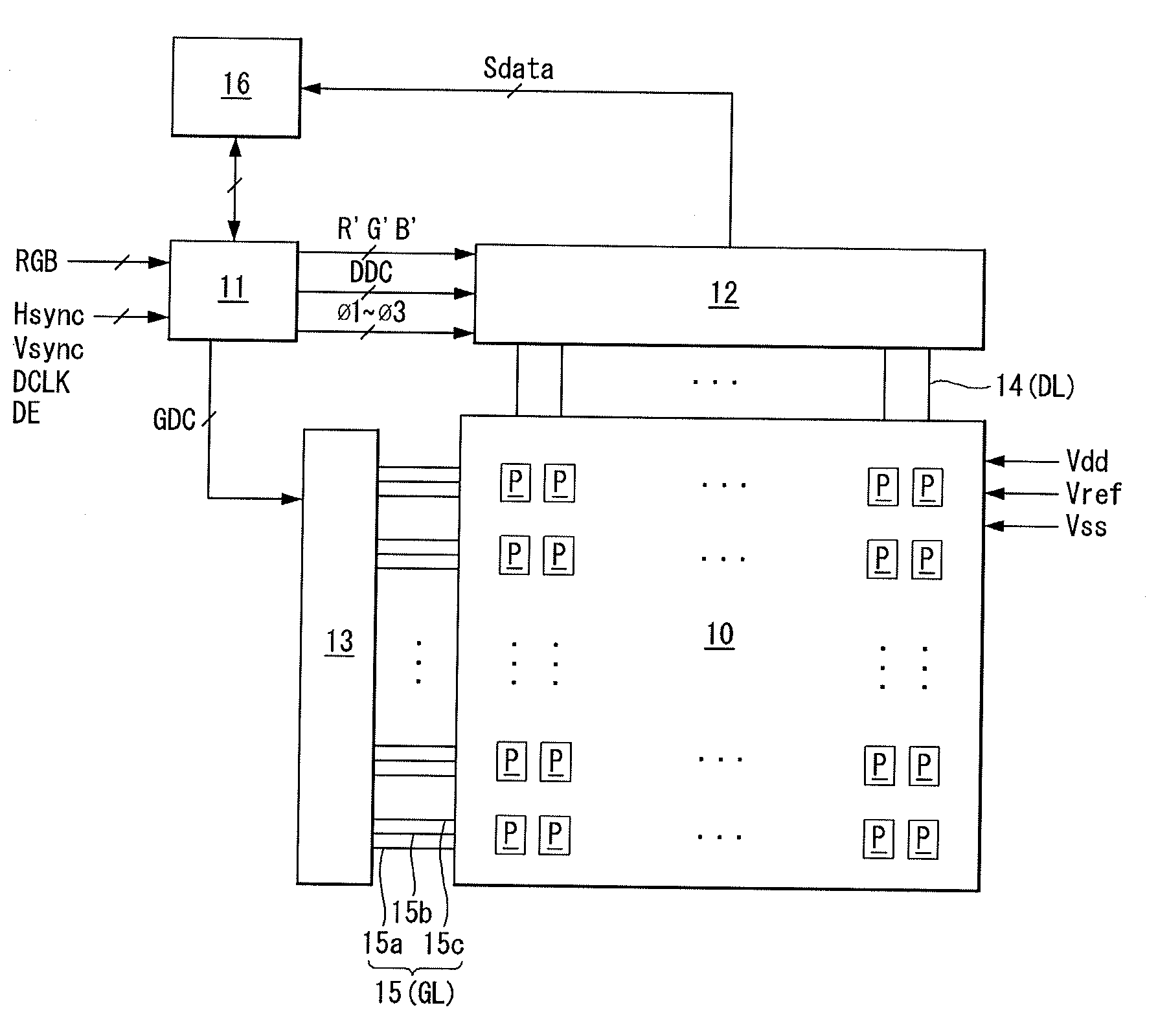
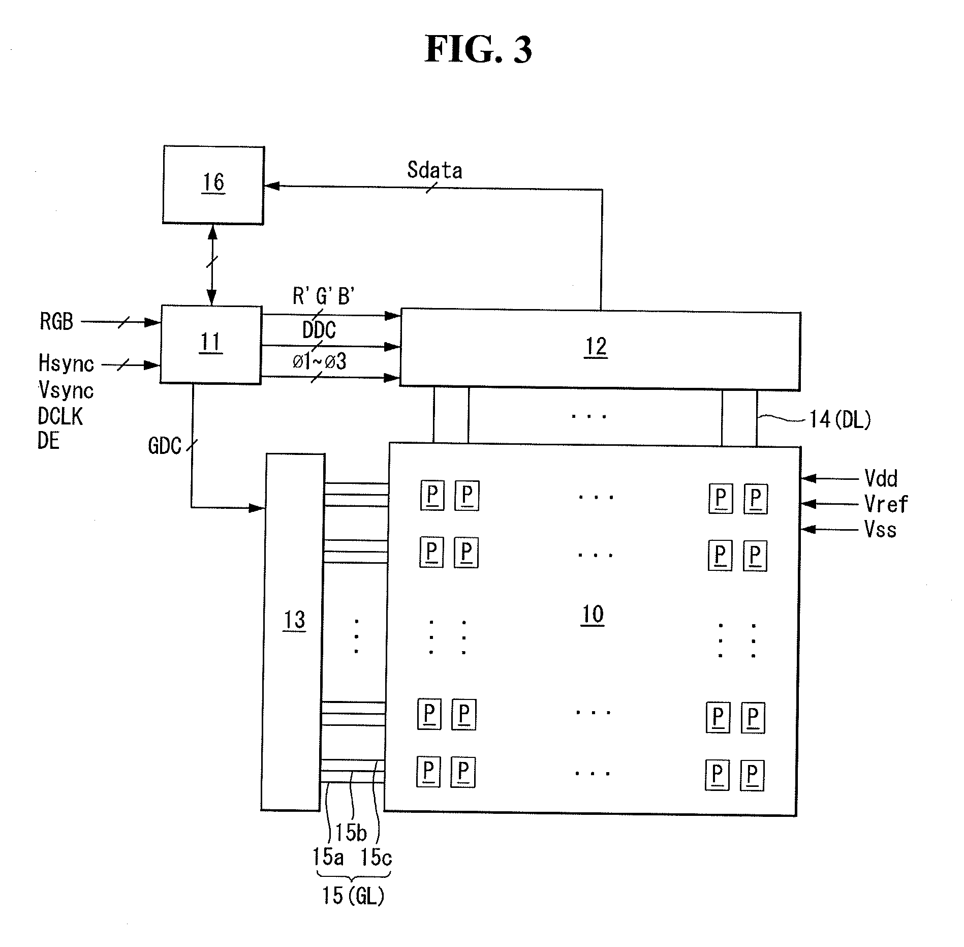
[0039]FIG. 3 is a view showing an organic light emitting diode display according to an exemplary embodiment of the present invention. FIG. 4 is a view showing in detail a data driving circuit of FIG. 3.

[0040]Referring to FIGS. 3 and 4, the organic light emitting diode display according to the exemplary embodiment of the present invention comprises a display panel 10 having pixels P arranged in a matrix, a data driving circuit 12 for driving data line portions 14, a gate driving circuit 13 for driving gate line portions 15, a timing controller for controlling the driving timings of the data driving circuit 12 and the gate driving circuit 13, and a memory 16.

[0041]In the display panel 10, a plurality of data line portions 14 and a plurality of gate line portions 15 intersect each other, and each of the intersections has the pixels P arranged in a matrix. Each of the data l...


PUM


Abstract

Disclosed are an organic light emitting diode display, which can reduce image sticking caused by the deterioration of an organic light emitting diode, and a driving method thereof. The organic light emitting diode display comprises: a display panel comprising a plurality of pixels arranged in a matrix at intersections of gate line portions and data line portions and each having an organic light emitting diode; a memory for storing compensation data; a timing controller for modulating input digital video data based on the compensation data and generating modulated data; and a data driving circuit for, during compensation driving, generating the compensation data to compensate for a difference in the deterioration of the organic light emitting diodes by supplying a sensing voltage to the pixels and sampling the threshold voltage of the organic light emitting diodes, which is fed back from the pixels, and for, during normal driving, converting the modulated data into a data voltage and supplying the data voltage to the pixels.

Description

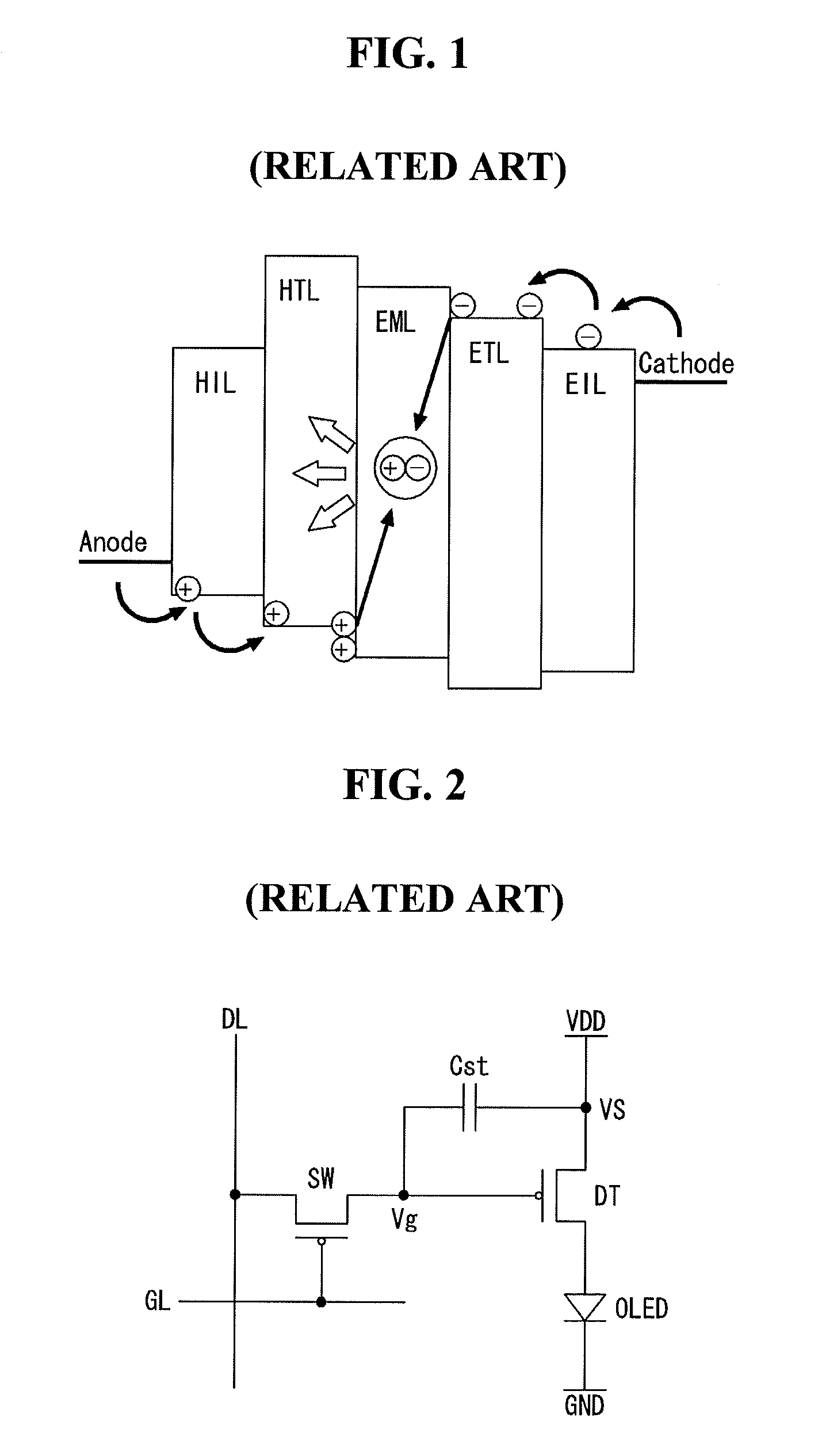
[0001]This application claims the benefit of Korea Patent Application No. 10-2009-0113979 filed on Nov. 24, 2009, which is incorporated herein by reference for all purposes as if fully set forth herein.BACKGROUND[0002]1. Field[0003]This document relates to an organic light emitting diode display, and more particularly, to an organic light emitting diode display, which can reduce image sticking caused by the deterioration of an organic light emitting diode, and a driving method thereof.[0004]2. Related Art[0005]Recently, organic light emitting diode displays spotlighted as display devices have the advantages of a rapid response speed, high emission efficiency, high luminance, and wide viewing angle by using a self-luminous device, which emits light by itself.[0006]An organic light emitting diode display has an organic light emitting diode as shown in FIG. 1. The organic light emitting diode is provided with organic compound layers HIL, HTL, EML, ETL, and EIL formed between an anode a...

Claims


Application Information

Patent Timeline
IPC IPC(8): G09G5/00
CPCG09G3/3233G09G2300/0842G09G2300/0861G09G2320/045G09G2320/0295G09G2320/043G09G2310/0262G09G3/20G09G3/30
Inventor BAE, HANJINKIM, BUMSIKJEONG, YUNSIKKIM, SEUNGTAE
Owner LG DISPLAY CO LTD
Learn More