Image pickup apparatus and radiation image pickup system
- Summary
- Abstract
- Description
- Claims
- Application Information
AI Technical Summary
Benefits of technology
Problems solved by technology
Method used
Image
Examples
first embodiment
[0022]FIG. 1 is a diagram schematically illustrating an image pickup apparatus according to a first embodiment of the present invention.
[0023]In FIG. 1, reference numeral 1 denotes a photoelectric conversion element, reference numerals 2 and 3 denote switch elements, reference numerals 4 and 5 denote gate wirings through which on / off-signals are transmitted to TFTs, and reference numeral 6 denotes a signal wiring. In the example shown in FIG. 1, a photodiode is used as the photoelectric conversion element 1, and a negative bias voltage is applied to the photodiode. That is, a cathode electrode of the photodiode is supplied with a positive bias voltage. A bias wiring 7 is used in common for a plurality of photodiodes and is connected to a power supply circuit Vs. A reset wiring 8 is used in common for the plurality of photodiodes and is connected to a power supply circuit Vr. As for the photoelectric conversion element 1, for example, a MIS-type or PIN-type thin-film photoelectric co...
second embodiment
[0033]FIG. 7 is a plan view illustrating 6×6 pixels of an image pickup apparatus according to a second embodiment, as seen from one side of an insulating substrate 21. The image pickup apparatus according to this embodiment is different from that according to the first embodiment in that vias 17 connected to gate wirings 4 and 5 are formed at different locations in the insulating substrate 21.
[0034]As shown in FIG. 7, one of the vias 17 is connected to a gate wiring 4 for transfer TFTs 2 and another one of the vias 17 is connected to a gate wiring 5 for reset TFTs 3. Each via 17 is disposed at the middle, as seen in the direction in which the gate wirings extend, of the corresponding gate wiring connected to a row of pixels (6 pixels in this embodiment). More specifically, in FIG. 7, vias 17 connected to gate wirings 4 and 5 are disposed at the middle of the area of the insulating substrate 21 occupied by each row of pixels.
[0035]FIG. 8 is a plan view of 6×6 pixels of the image pick...
third embodiment
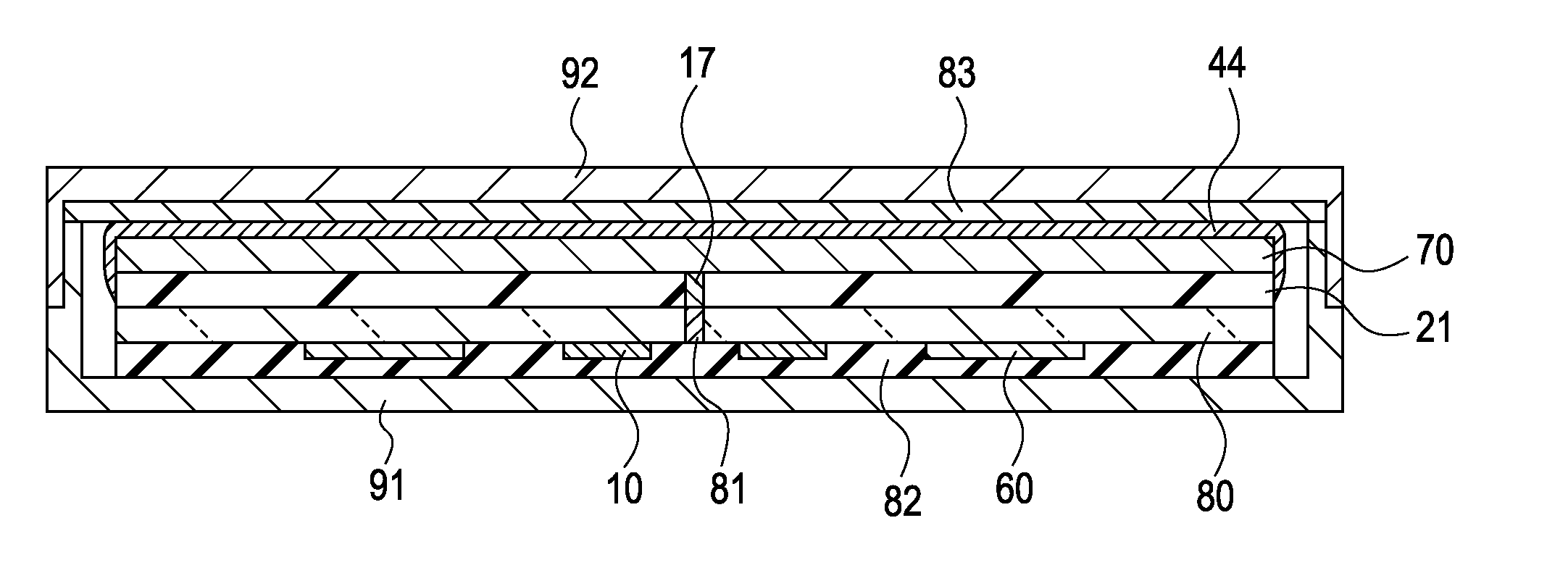
[0038]FIG. 9 is a cross-sectional view of an image pickup apparatus having a two-part housing according to a third embodiment of the invention.
[0039]In FIG. 9, reference numeral 70 denotes a conversion unit including transfer and reset TFTs, photoelectric conversion elements, and scintillators (not shown) arranged on an insulating substrate 21. Reference numeral 80 denotes a circuit board on which a gate driving circuit 10, a signal processing circuit 60, etc. are disposed. Reference numeral 81 denotes a via formed in the circuit board 80. Reference numeral 82 denotes an insulating layer having thermal conductivity covering the circuit board 80. Reference numeral 83 denotes a protective layer. Reference numerals 91 and 92 denote two parts of the housing.
[0040]The via 81 of the circuit board 80 is connected to a via 17 formed in the insulating substrate 21. In the example shown in FIG. 9, the via 81 of the circuit board 80 is formed in the shape of a through-hole. In a case where an ...
PUM
 Abstract
Description
Claims
Application Information
 - R&D
- Intellectual Property
- Life Sciences
- Materials
- Tech Scout
- Unparalleled Data Quality
- Higher Quality Content
- 60% Fewer Hallucinations
Browse by: Latest US Patents, China's latest patents, Technical Efficacy Thesaurus, Application Domain, Technology Topic, Popular Technical Reports.
© 2025 PatSnap. All rights reserved.Legal|Privacy policy|Modern Slavery Act Transparency Statement|Sitemap|About US| Contact US: help@patsnap.com


