Transceiver system, semiconductor device thereof, and data transceiving method of the same

a technology of transceiver and semiconductor device, applied in the direction of logic circuit coupling/interface, pulse technique, instruments, etc., can solve the problem that the capacitor component may limit the high-speed operation of a multi-stack package semiconductor devi

Active Publication Date: 2011-03-10
SAMSUNG ELECTRONICS CO LTD
View PDF14 Cites 2 Cited by
  • Summary
  • Abstract
  • Description
  • Claims
  • Application Information

AI Technical Summary

Benefits of technology

[0020]The semiconductor device may be a semiconductor memory device further including a memory cell array and a decoder/selector. The memory cell array may be configured to receive and store the input signal during a write operation, and output an output signal during a read operation. The decoder/selector may be configured to output a control signal of a low level in response to a command signal input from the outside during the read operation, output the control signal of a high level during a refresh operation, and output the control signal in response to the output signal during the write operation. The terminator/driver may include: a PMOS transistor connected with the supply voltage and to which the control signal is applied and a pull-up resistor connected between the PMOS transistor and the I/O pad.
[0021]According to an exemplary embodiment of the inventive concept, a data transceiving method of a semiconductor device includes a first semiconductor device having a first I/O pad connected with an I/O channel, and a second semiconductor device having a second I/O pad connected with the I/O channel. The method includes terminating, by the first semiconductor device, the first I/O pad with a first voltage when the second semiconductor device transmits data to the first semiconductor device, terminating, by the second semiconductor device, the second I/O pad with a second voltage higher than the first voltage when the first semiconductor device transmits data to the second semiconductor device,

Problems solved by technology

Such an input capacitance component may limit high-speed operation of a multi-stack package semiconductor device in which a plurality of semiconductor chips are stacked to improve the degree of integration.

Method used


Image

  • Transceiver system, semiconductor device thereof, and data transceiving method of the same
  • Transceiver system, semiconductor device thereof, and data transceiving method of the same
  • Transceiver system, semiconductor device thereof, and data transceiving method of the same

Examples


Embodiment Construction

[0031]The inventive concept will now be described more fully with reference to the accompanying drawings in which some exemplary embodiments are shown. This inventive concept, however, may be embodied in many alternate forms and should not be construed as limited to only the exemplary embodiments set forth herein. Like numbers refer to like elements throughout the description of the figures. It will be understood that when an element is referred to as being “connected” or “coupled” to another element, it can be directly connected or coupled to the other element or intervening elements may be present.

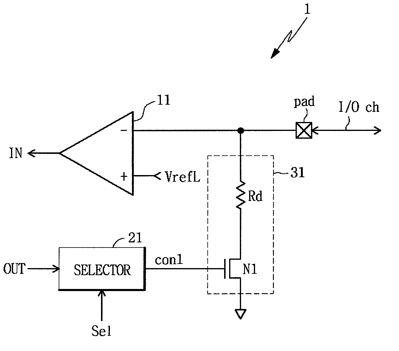
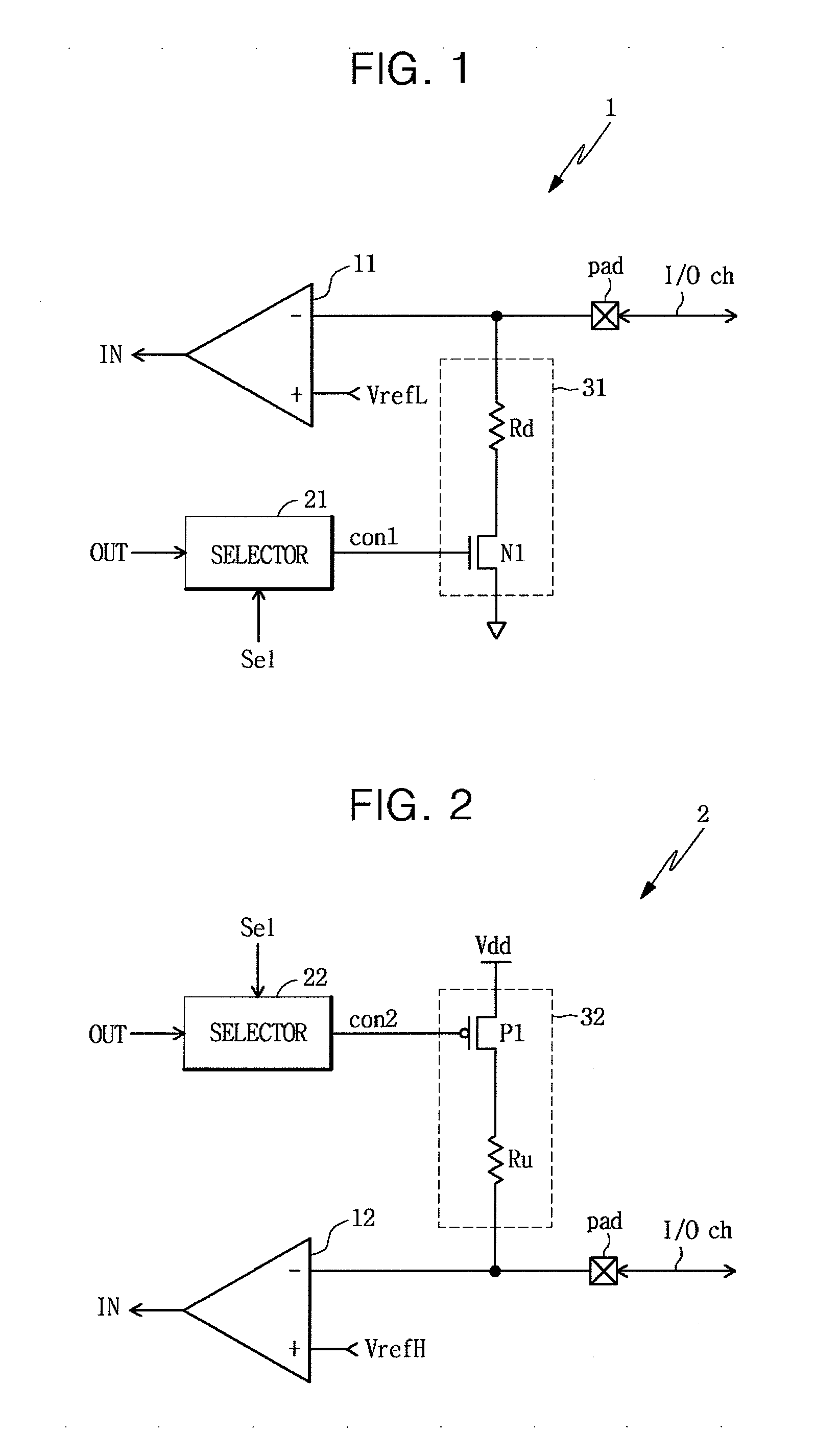
[0032]FIG. 1 illustrates an input / output (I / O) circuit 1 of a semiconductor device according to an exemplary embodiment of the inventive concept. The I / O circuit 1 may include an input unit 11, a selector 21, a terminator / driver 31, and an I / O pad pad. The terminator / driver 31 may include a pull-down resistor Rd and a pull-down circuit. The pull-down circuit may be an n-type metal oxide ...


PUM


Abstract

A transceiver system includes a first semiconductor device having a first input / output (I / O) pad connected with an I / O channel and a second semiconductor device having a second I / O pad connected with the I / O channel. The first semiconductor device is configured to terminate the first I / O pad with a first voltage when data is received, and maintain the first I / O pad and the I / O channel at the first voltage when data is transmitted. The second semiconductor device is configured to terminate the second I / O pad with a second voltage higher than the first voltage when data is received, and maintain the second I / O pad and the I / O channel at the second voltage when data is transmitted.

Description

CROSS-REFERENCE TO RELATED APPLICATION[0001]This application claims priority under 35 U.S.C. §119 to Korean Patent Application No. 10-2009-85456, filed on Sep. 10, 2009, the disclosure of which is incorporated by reference in its entirety herein.BACKGROUND[0002]1. Technical Field[0003]Exemplary embodiments of the inventive concept relate to a transceiver system, and more particularly, to a semiconductor device having an input / output (I / O) circuit capable of transceiving data, a transceiver system having the semiconductor device, and a data transceiving method of the transceiver system.[0004]2. Discussion of Related Art[0005]A semiconductor device can transceive signals with another semiconductor device through a channel. The semiconductor device may include an I / O circuit connected with the channel to transceive the signals. The I / O circuit may be used to transmit signals through a channel and receive signals through the channel to restore signals.[0006]The I / O circuit may include a...

Claims


Application Information

Patent Timeline
IPC IPC(8): H03K19/003
CPCG11C7/1051G11C7/1057H03K19/018514G11C7/1084H03K19/01759G11C7/1078G11C7/10G11C11/4093
Inventor CHOI, SEOK-WOO
Owner SAMSUNG ELECTRONICS CO LTD
Why Eureka
Try Eureka