
Semiconductor Device Including Fuse Having Form of Capacitor

Active Publication Date: 2011-03-03
SAMSUNG ELECTRONICS CO LTD
View PDF1 Cites 3 Cited by
  • Summary
  • Abstract
  • Description
  • Claims
  • Application Information

AI Technical Summary

Benefits of technology

[0007]The inventive concept provides a semiconductor device including a fuse in which an additional process of forming a fuse is not required and spatial efficiency may be achieved.

Problems solved by technology

Furthermore, the area of the fuse is large, and thus in a highly-integrated memory device, the fuse is inefficient with respect to the usage of space.

Method used


Image

  • Semiconductor Device Including Fuse Having Form of Capacitor
  • Semiconductor Device Including Fuse Having Form of Capacitor
  • Semiconductor Device Including Fuse Having Form of Capacitor

Examples


Embodiment Construction

[0037]Exemplary embodiments of the inventive concept will now be described more fully with reference to the accompanying drawings. The inventive concept may, however, be embodied in many different forms and should not be construed as being limited to the exemplary embodiments set forth herein.

[0038]The terminology used herein is for the purpose of describing particular embodiments only and is not intended to be limiting of the invention.

[0039]Hereinafter, exemplary embodiments of the inventive concept will be described with reference to accompanying drawings. In the drawings, for example, illustrated shapes may be deformed according to fabrication technology and / or tolerances. Therefore, the exemplary embodiments of the inventive concept are not limited to certain shapes illustrated in the present specification, and may include modifications of shapes caused in fabrication processes.

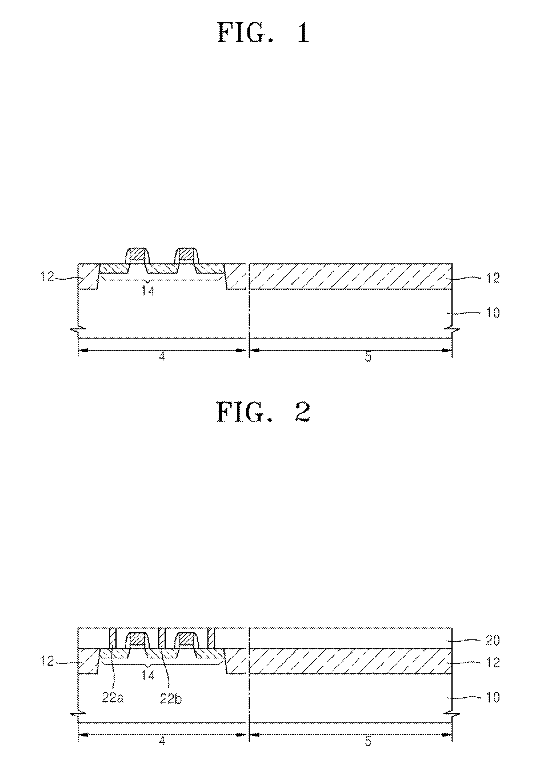
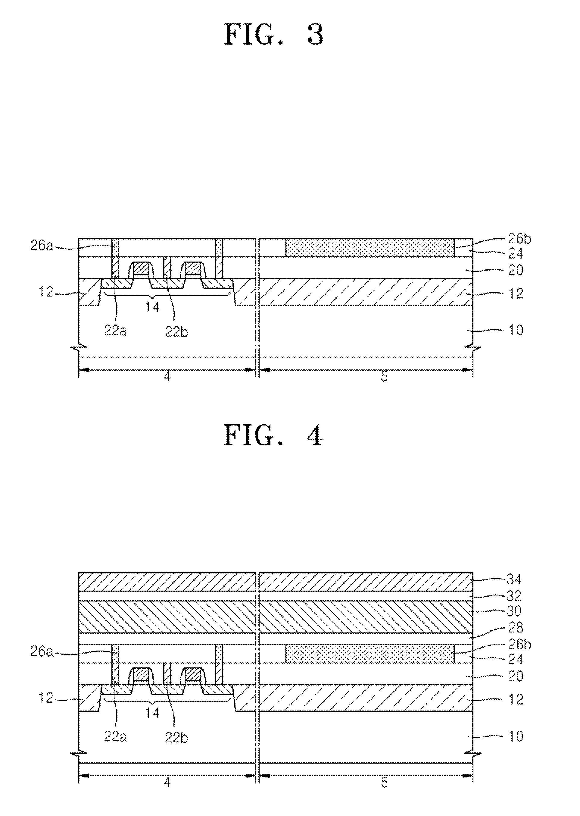
[0040]FIGS. 1 through 11 are cross-sectional views of a semiconductor device that is manufactured acc...


PUM


Abstract

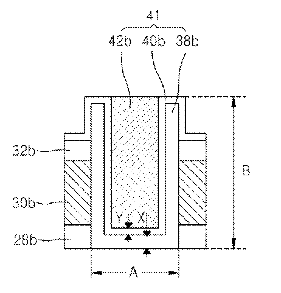
A semiconductor device includes a fuse having the form of a capacitor. The semiconductor device includes a cathode formed on a semiconductor substrate, an anode formed over the cathode, and at least one filament having a cylindrical-shell shape formed between the cathode and the anode and electrically connecting the cathode and the anode.

Description

CROSS-REFERENCE TO RELATED APPLICATIONS[0001]This application claims the benefit of Korean Patent Application No. 10-2009-0081980, filed on Sep. 1, 2009, in the Korean Intellectual Property Office, the disclosure of which is incorporated herein in its entirety by reference.BACKGROUND[0002]1. Technical Field[0003]The inventive concept relates to a semiconductor device including a fuse, and more particularly, to a semiconductor device including a fuse having the form of a capacitor.[0004]2. Discussion of the Related Art[0005]In the fabrication of semiconductor memory devices, it is common to have a memory device with one or more defective memory cells. Rather than discarding the entire memory device, defective memory cells may usually be replaced by redundant memory cells that are included in the memory device for this very purpose. In this case, the defective memory cells may be electrically insulated from other memory cells by cutting conductive filaments with a laser or the like, o...

Claims


Application Information

Patent Timeline
IPC IPC(8): H01L29/86
CPCH01L23/5256H01L27/10894H01L27/10852H01L27/105H01L2924/0002H10B12/033H10B12/09H01L2924/00H01L23/62
Inventor SONG, HO-JUKIM, SEONG-HOPARK, WON-MOKIM, GIL-SUB
Owner SAMSUNG ELECTRONICS CO LTD
Learn More