Housing for electronic device and method for making the same
a technology for electronic devices and housings, applied in the direction of electric apparatus casings/cabinets/drawers, gaseous cathodes, gas-filled discharge tubes, etc., can solve problems such as hard to touch
- Summary
- Abstract
- Description
- Claims
- Application Information
AI Technical Summary
Problems solved by technology
Method used
Image
Examples
Embodiment Construction
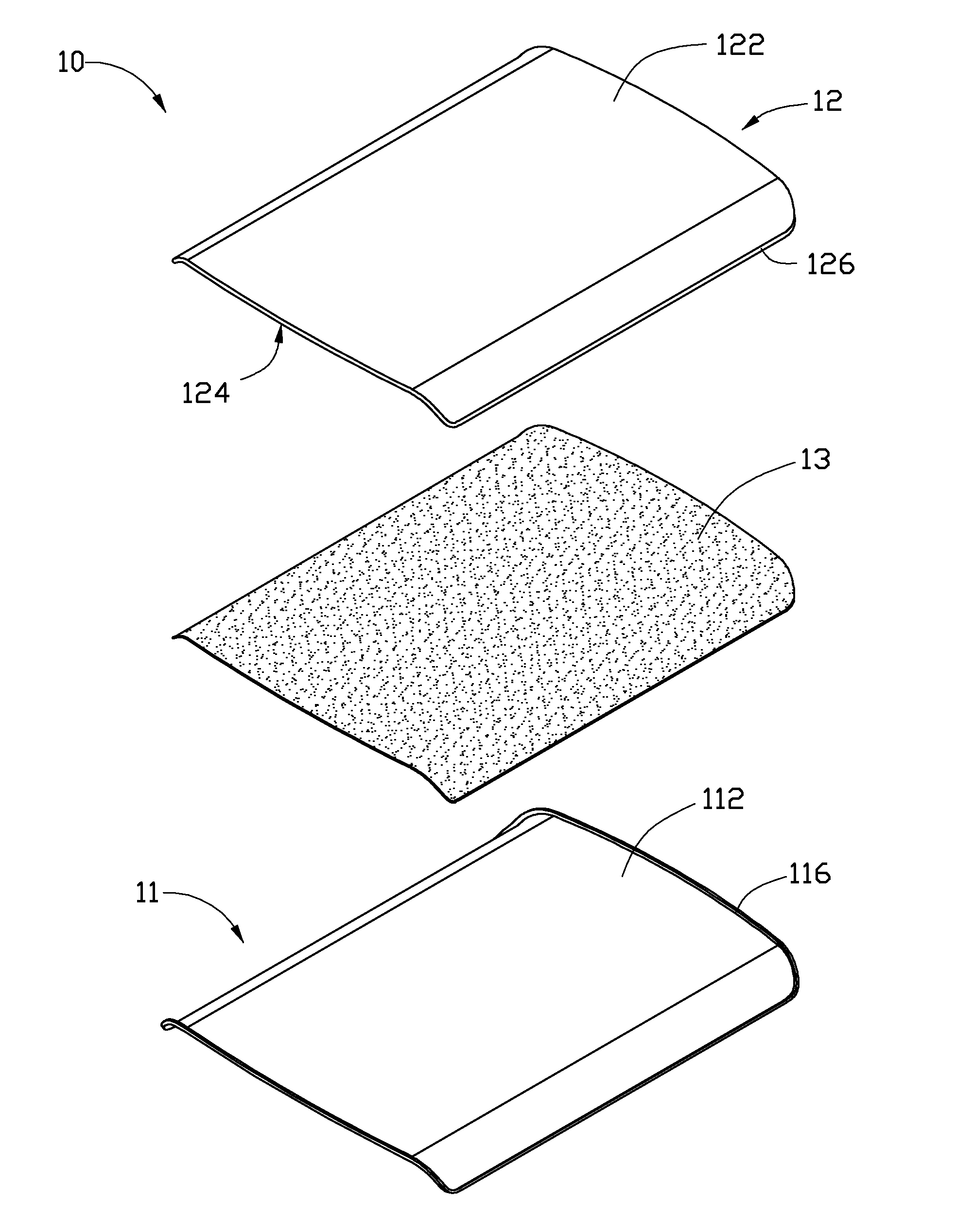
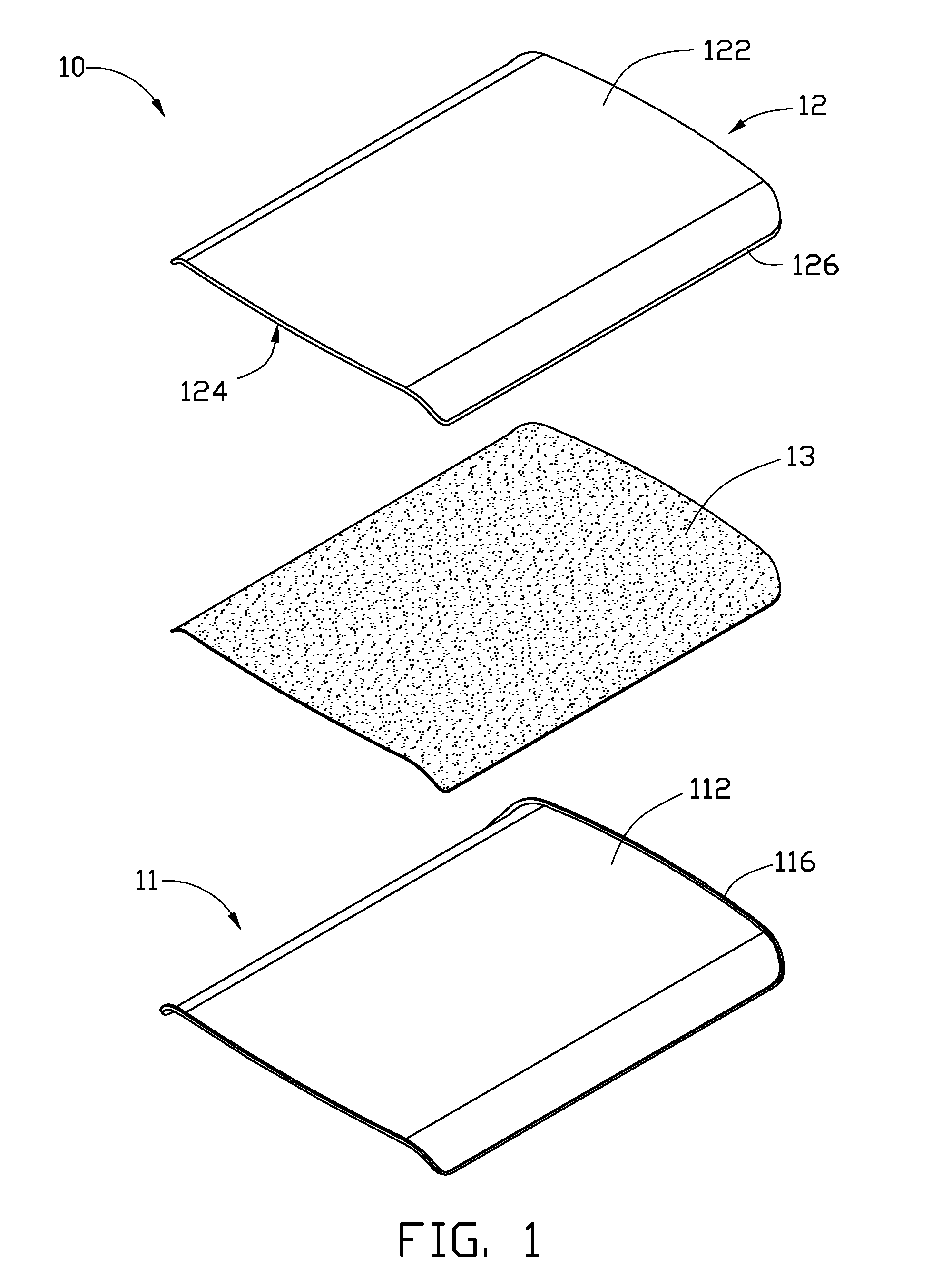
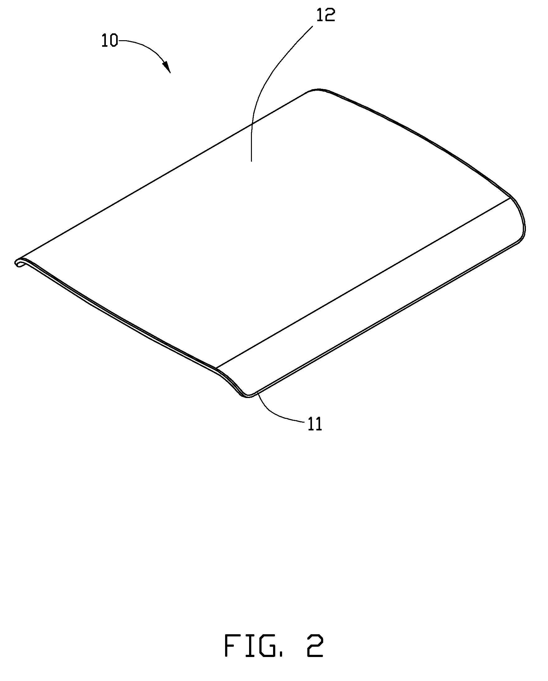
[0010]FIG. 1 and FIG. 3 show an exemplary housing 10 for an electronic device such as a mobile phone. The housing 10 includes a substrate 11, and a soft layer 12 bonded to the substrate 11 by an adhesive layer 13.
[0011]The substrate 11 can be made of metal, such as stainless steel, magnesium alloy, aluminum alloy, titanium alloy etc. The substrate 11 has a bonding surface 112, a peripheral edge 114, and a ridge 116 protruding from the peripheral edge 114 and surrounding the bonding surface 112. The bonding surface 112 may be roughened (e.g., by etching or grinding) facilitating a good bonding of the soft layer 12 to the substrate 11. The ridge 116 has an end surface 1162 (best shown in FIG. 3) extends from the peripheral edge 114. The length of the ridge 116 from peripheral edged 114 to the end surface 1162 is about equal to the combined thickness of the soft layer 12 and the adhesive layer 13.
[0012]The soft layer 12 is comprised of a material that is soft to the touch. Exemplary ma...
PUM
| Property | Measurement | Unit |
|---|---|---|
| Pressure | aaaaa | aaaaa |
| Adhesivity | aaaaa | aaaaa |
Abstract
Description
Claims
Application Information
 - R&D
- Intellectual Property
- Life Sciences
- Materials
- Tech Scout
- Unparalleled Data Quality
- Higher Quality Content
- 60% Fewer Hallucinations
Browse by: Latest US Patents, China's latest patents, Technical Efficacy Thesaurus, Application Domain, Technology Topic, Popular Technical Reports.
© 2025 PatSnap. All rights reserved.Legal|Privacy policy|Modern Slavery Act Transparency Statement|Sitemap|About US| Contact US: help@patsnap.com


