
Electronic module with feed through conductor between wiring patterns

a technology of electrical modules and wiring patterns, applied in the field of electrical modules, can solve the problems of increasing manufacturing time and cost, unreliable, and insufficiently reducing the size of necessary, so as to improve routing efficiency, reduce price, and thin structure

Active Publication Date: 2010-12-09
IMBERATEK LLC
View PDF45 Cites 17 Cited by
  • Summary
  • Abstract
  • Description
  • Claims
  • Application Information

AI Technical Summary

Benefits of technology

The invention allows for the creation of thin structures where semiconductor components are protected within a base. This results in mechanically durable and reliable joints between the circuit board and the semiconductor components. The invention also improves routing efficiency and reduces costs, especially when increasing the number of contacts and narrowing the pitch between contact lands on the component.

Problems solved by technology

The technical problem addressed in this patent is the need for improved methods and technologies to make electrical connections between two sides of a wiring board with through holes that have high routing efficiency and are cost-effective. The current methods, such as chemical and electroplating, have limitations in achieving reliable conductive micro vias with aspect ratio greater than 1.00 and in narrow and deep through holes or micro vias having a diameter of 150 μm or less. The background art also contains different solutions that do not adequately provide high routing efficiency with an affordable price of the product.

Method used


Image

  • Electronic module with feed through conductor between wiring patterns
  • Electronic module with feed through conductor between wiring patterns
  • Electronic module with feed through conductor between wiring patterns

Examples


first embodiment

[0109]The pre-assembled body 250 can be done by various ways, confer the description of the first embodiment and FIG. 3A.

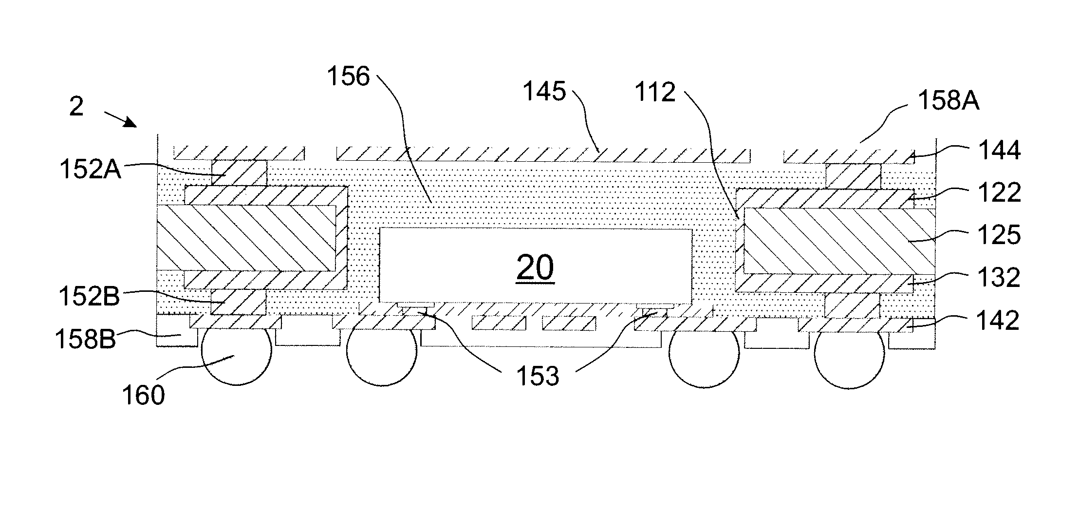
[0110]FIG. 5B presents a cross profile view of a readymade electronic module 3 including feed through conductor component 200 according to an embodiment of the invention manufactured by the second method. The feed through conductor component 200 is located substantially in the middle of the electronic module package 3. The electronic module 3 contains an embedded component 30 which is connected by microvias 253 to the third wiring layer 242. The fourth wiring layer 244 may also contain a functional feature 245 such like EMI shield or ground, for instance. The embedded component 30 is surrounded on all other sides than the third wiring layer 242 by an insulation material such as cured prepreg layers 256.

[0111]FIGS. 6A-6I present a third method for manufacturing a feed through conductors according to an embodiment of the invention. All of the FIGS. 6A-6I comprise a ...

third embodiment

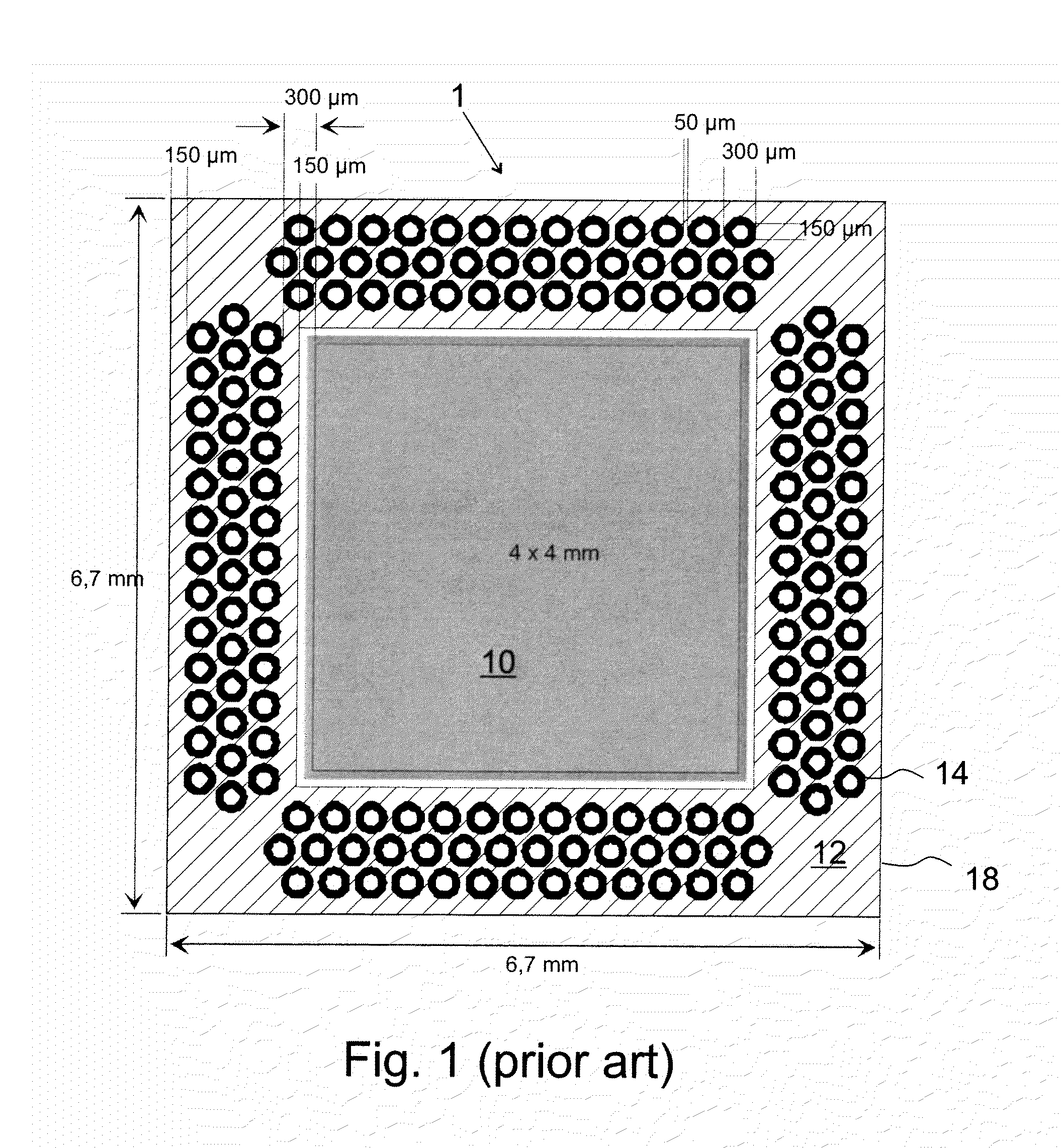
[0137]FIG. 9A presents an example of mechanically routing finished feed through conductors according to the invention. As an example of typical mechanic routing is done in the middle of the conductors running on top or bottom surface part of the dielectric to make an opening in a vertical conductor part 61. In FIG. 9D is presented another type of routing which conforms a L-type of feed through conductor. In the current routing means a typical value for a line width 67 is approximately 50 μm and for a space is approximately 150 μm. In advanced embodiments the respective values are 40 μm and 100 μm, for instance. The pitch 63 for typical embodiments is approximately 200 μm and advanced embodiments 140 μm.

[0138]FIG. 9B presents an example of mechanically drilling finished feed through conductors according to the third embodiment of the invention. As an example, a typical mechanic drilling is done in the middle of the conductors running on top or bottom surface part of the dielectric to...


PUM


Abstract

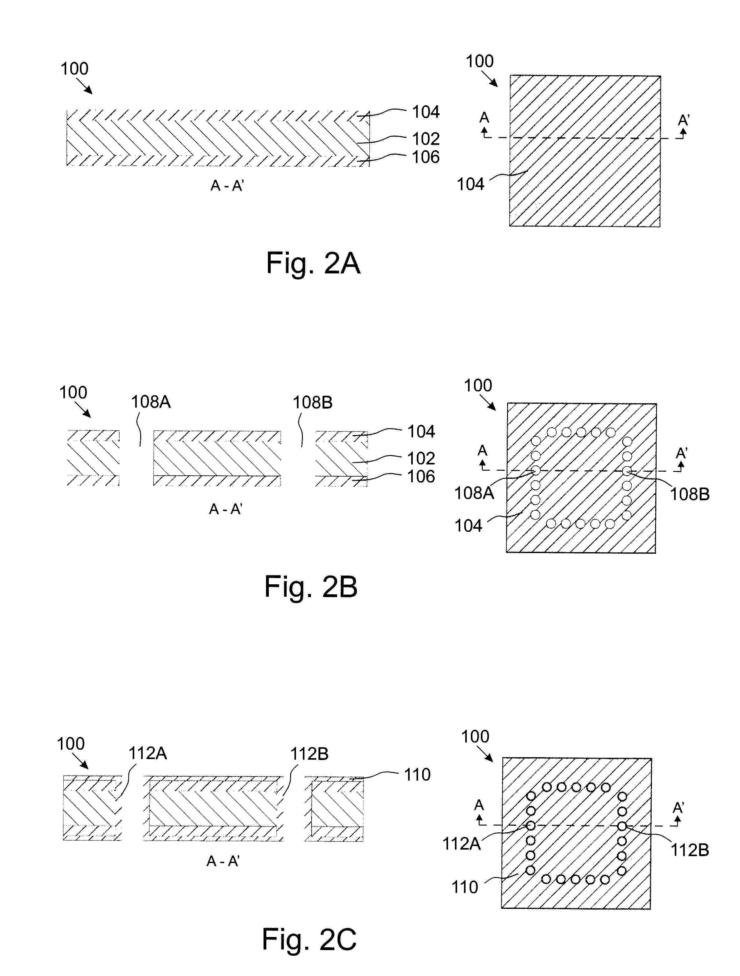
The electronic module comprises a dielectric 1031 substrate having a first surface and a second surface and an installation cavity extending through the dielectric substrate and having a perimetrical side wall. The electronic module further comprises a first wiring layer 1032 on the first surface, a second wiring layer 1033 on the second surface, and a feed through conductor 1034 on the perimetrical side wall and electrically connecting at least one conductor in the first wiring layer to at least one conductor in the second wiring layer. There is also at least one IC inside the installation cavity. The electronic module further comprises a first insulating layer 1035 on the second wiring layer, a second insulating layer 1036 on the first wiring layer, and a third wiring layer 1037 on the first insulating layer. First microvias 1038 inside the first insulating layer make electrical connections between the second wiring layer and the third wiring layer. Second microvias 1039 electrically connect the IC to at least one of the second wiring layer and the third wiring layer. The electronic module comprises also a fourth wiring layer 1040 on the second insulating layer and third microvias 1041 inside the second insulating layer and making electrical connections between the first wiring layer and the fourth wiring layer.

Description


Claims


Application Information

Patent Timeline
Owner IMBERATEK LLC
Learn More