
Method and apparatus for manufacturing semiconductor device

Active Publication Date: 2010-06-24
JUSUNG ENG
View PDF3 Cites 4 Cited by
  • Summary
  • Abstract
  • Description
  • Claims
  • Application Information

AI Technical Summary

Benefits of technology

[0015]Another object of the present invention is to provide a method and apparatus for manufacturing a semiconductor device, which is capable of realizing an extension of a cleaning cycle for a processing chamber, and improving an interfacial property of a thin film formed on a substrate.

Problems solved by technology

However, since the inside of the processing chamber can not be cleaned only with the dry cleaning method, a wet cleaning method has to be additionally used to perfectly clean the inside of the processing chamber after disjointing the processing chamber by a worker.
However, if cleaning the inside of the processing chamber by the wet cleaning method, the apparatus including the processing chamber to be cleaned has to be turned off.
Furthermore, a step for checking a uniformity of thin film and a pollution level of particles has to be inevitably made by applying a virtual deposition process to a dummy substrate, which causes the waste of time and low yield.

Method used


Image

  • Method and apparatus for manufacturing semiconductor device
  • Method and apparatus for manufacturing semiconductor device
  • Method and apparatus for manufacturing semiconductor device

Examples


first embodiment

[0053]FIG. 5 illustrates an apparatus for manufacturing a semiconductor device according to the present invention.

[0054]Referring to FIG. 5, the apparatus for manufacturing the semiconductor device according to the first embodiment of the present invention has a cluster-type arrangement structure, which comprises a substrate-transferring chamber 100, a load-lock chamber 200, a preheating chamber 300, and a plurality of processing chambers 400, 410, 420, 430, and 440.

[0055]The substrate-transferring chamber 100 is positioned at the central part surrounded by the respective chambers, wherein the substrate-transferring chamber 100 transfers the substrate to the respective chambers. For this, the substrate-transferring chamber 100 includes a substrate-transferring unit 110 for transferring the substrate to the respective chambers. The substrate-transferring chamber 100 is surrounded by the load-lock chamber 200, the preheating chamber 300, and the plurality of processing chambers 400, 4...

second embodiment

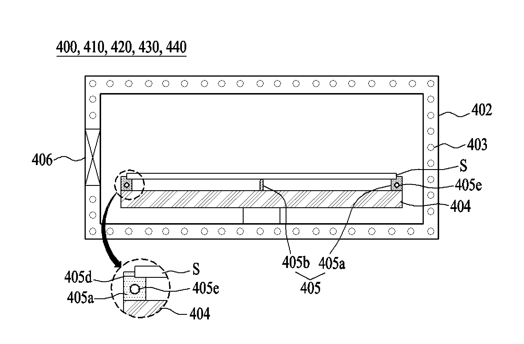
[0065]As shown in FIG. 8, each of the processing chambers 400, 410, 420, 430, and 440 according to the present invention may comprise a chamber wall 402, a thermal-insulating member 403, and a susceptor 404.

[0066]The chamber wall 402 is arranged in communication with the substrate-transferring chamber 100, and the chamber wall 402 prepares a reaction space for the thin-film deposition process. Also, a door 406 is provided at one side of the chamber wall 402 so that the substrate can be easily loaded into or unloaded from each processing chamber through the door 406.

[0067]The thermal-insulating member 403 is provided in the chamber wall 402, so that the inner temperature of each of the processing chambers 400, 410, 420, 430, and 440 is constantly maintained within a range between the atmospheric temperature and the temperature of the preheated substrate (S). At this time, the thermal-insulating member 403 may be a heating coil or heating pipe.

[0068]The susceptor 404 is elevated by a ...

third embodiment

[0069]As shown in FIG. 9, each of the processing chambers 400, 410, 420, 430, and 440 according to the present invention may comprise a chamber wall 402, a thermal-insulating member 403, a susceptor 404, and a substrate-supporting unit 405.

[0070]The chamber wall 402 is arranged in communication with the substrate-transferring chamber 100, and the chamber wall 402 prepares a reaction space for the thin-film deposition process. Also, a door 406 is provided at one side of the chamber wall 402 so that the substrate can be easily loaded into or unloaded from each processing chamber through the door 406.

[0071]The thermal-insulating member 403 is provided in the chamber wall 402, so that the inner temperature of each of the processing chambers 400, 410, 420, 430, and 440 is constantly maintained within a range between the atmospheric temperature and the temperature of the preheated substrate (S). At this time, the thermal-insulating member 403 may be a heating coil or heating pipe.

[0072]Th...


PUM

PropertyMeasurementUnit
Timeaaaaaaaaaa
Temperatureaaaaaaaaaa
Lengthaaaaaaaaaa

Abstract

A method and apparatus for manufacturing a semiconductor device is disclosed, which is capable of realizing an extension of a cleaning cycle for a processing chamber, the method comprising preheating a substrate; placing the preheated substrate onto a substrate-supporting unit provided in a susceptor while the preheated substrate is maintained at a predetermined height from an upper surface of the susceptor provided in a processing chamber; and forming a thin film on the preheated substrate, wherein a temperature of the preheated substrate is higher than a processing temperature for forming the thin film in the processing chamber.

Description

CROSS REFERENCE TO RELATED APPLICATIONS[0001]This application claims the benefit of the Korean Patent Application Nos. P2008-0129158 filed on Dec. 18, 2008, and P2009-0108069 filed on Nov. 10, 2009, which are hereby incorporated by reference as if fully set forth herein.BACKGROUND OF THE INVENTION[0002]1. Field of the Invention[0003]The present invention relates to a method and apparatus for manufacturing a semiconductor device, and more particularly, to a method and apparatus for manufacturing a semiconductor device, which is capable of realizing an extension of a cleaning cycle for a processing chamber.[0004]2. Discussion of the Related Art[0005]Generally, a semiconductor device, a solar cell, a liquid crystal display device, and a light-emitting display device are manufactured by semiconductor-manufacturing steps including a thin-film deposition process, a photo process, an etching process, and a diffusion process.[0006]The thin-film deposition process may use a physical vapor de...

Claims


Application Information

Patent Timeline
IPC IPC(8): H01L21/365H01L21/36H01L21/363
CPCC23C16/0209C23C16/407C23C16/56H01L21/6875H01L21/02658H01L21/67103H01L21/67109H01L21/02554
Inventor PARK, SANG KIHWANG, SEONG RYONGCHO, GEUN TAE
Owner JUSUNG ENG
Learn More