ESD protection device and composite electronic component of the same
a protection device and electronic component technology, applied in the direction of overvoltage protection resistors, emergency protection arrangements for limiting excess voltage/current, magnetic bodies, etc., can solve the problems of significant variation in increase the starting voltage of the discharge, and degrade the signal quality, so as to improve the durability, improve the effect of heat resistance and weather resistance and improve productivity
- Summary
- Abstract
- Description
- Claims
- Application Information
AI Technical Summary
Benefits of technology
Problems solved by technology
Method used
Image

Examples
first embodiment
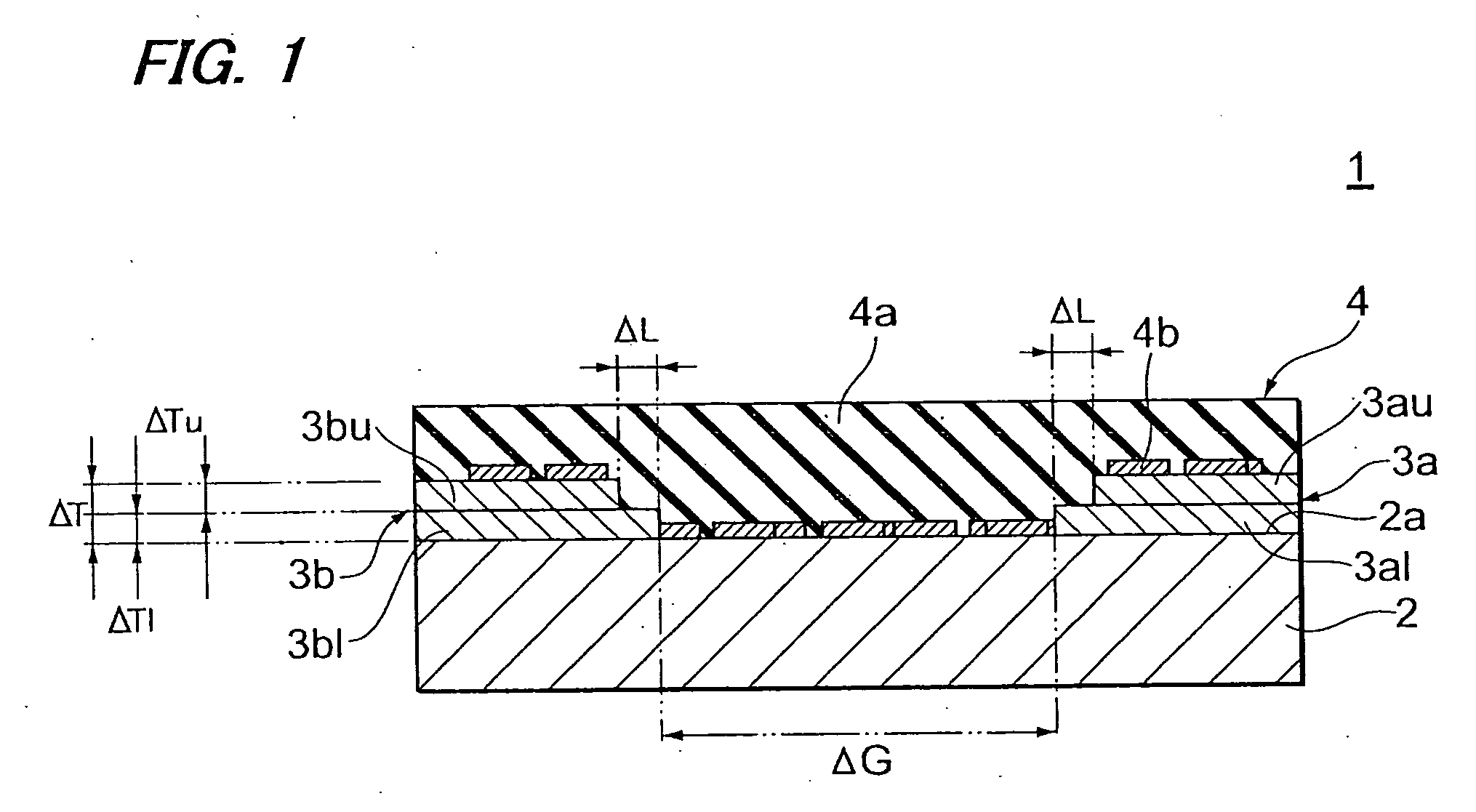
[0040]FIG. 1 is a schematic sectional view schematically showing a preferred embodiment of an ESD protection device according to the present invention. An ESD protection device 1 includes a base 2 having an insulating surface 2a, paired electrodes 3a and 3b disposed on the insulating surface 2a, a functional layer 4 disposed between the electrodes 3a and 3b, and a terminal electrode 5 (not shown in the drawings) electrically connected to the electrodes 3a and 3b. In the ESD protection device 1, the functional layer 4 is designed to function as an electrostatic protection material of a low voltage discharge type so that when overvoltage such as static electricity is applied to the ESD protection device 1, initial discharge occurs between the electrodes 3a and 3b via the functional layer 4.
[0041]The base 2 has the insulating surface 2a. Here, the base 2 having the insulating surface 2a is a concept including, besides a substrate composed of an insulating material, a substrate with an ...
second embodiment
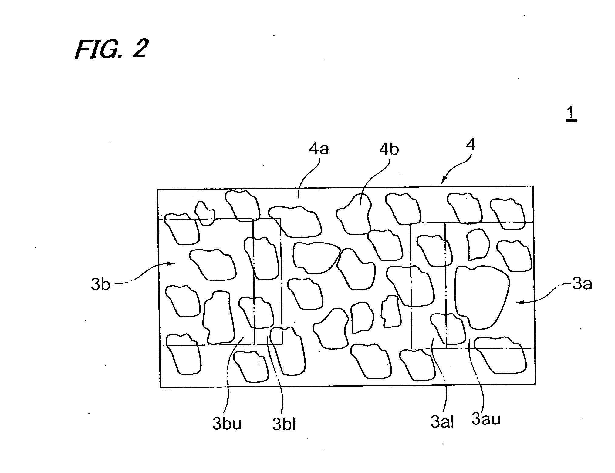
[0062]FIG. 3 is a schematic sectional view schematically showing another preferred embodiment of the ESD protection device according to the present invention. This ESD protection device 6 has the same configuration as that of the above-described ESD protection device 1 according to the first embodiment except that the ESD protection device 6 has a functional layer 7 instead of the functional layer 4.
[0063]The functional layer 7 is a composite in which conductive inorganic materials 4b (not shown in the drawings) are dispersed in a matrix of an insulating inorganic material 4a (not shown in the drawings). In the present embodiment, the functional layer 7 is formed by sputtering a target containing the insulating inorganic material 4a (or a target containing the insulating inorganic material 4a and the conductive inorganic materials 4b) onto an insulating surface 2a of a base 2 and / or electrodes 3a and 3b and then applying a voltage to between the electrodes 3a and 3b to allow part of...
third embodiment
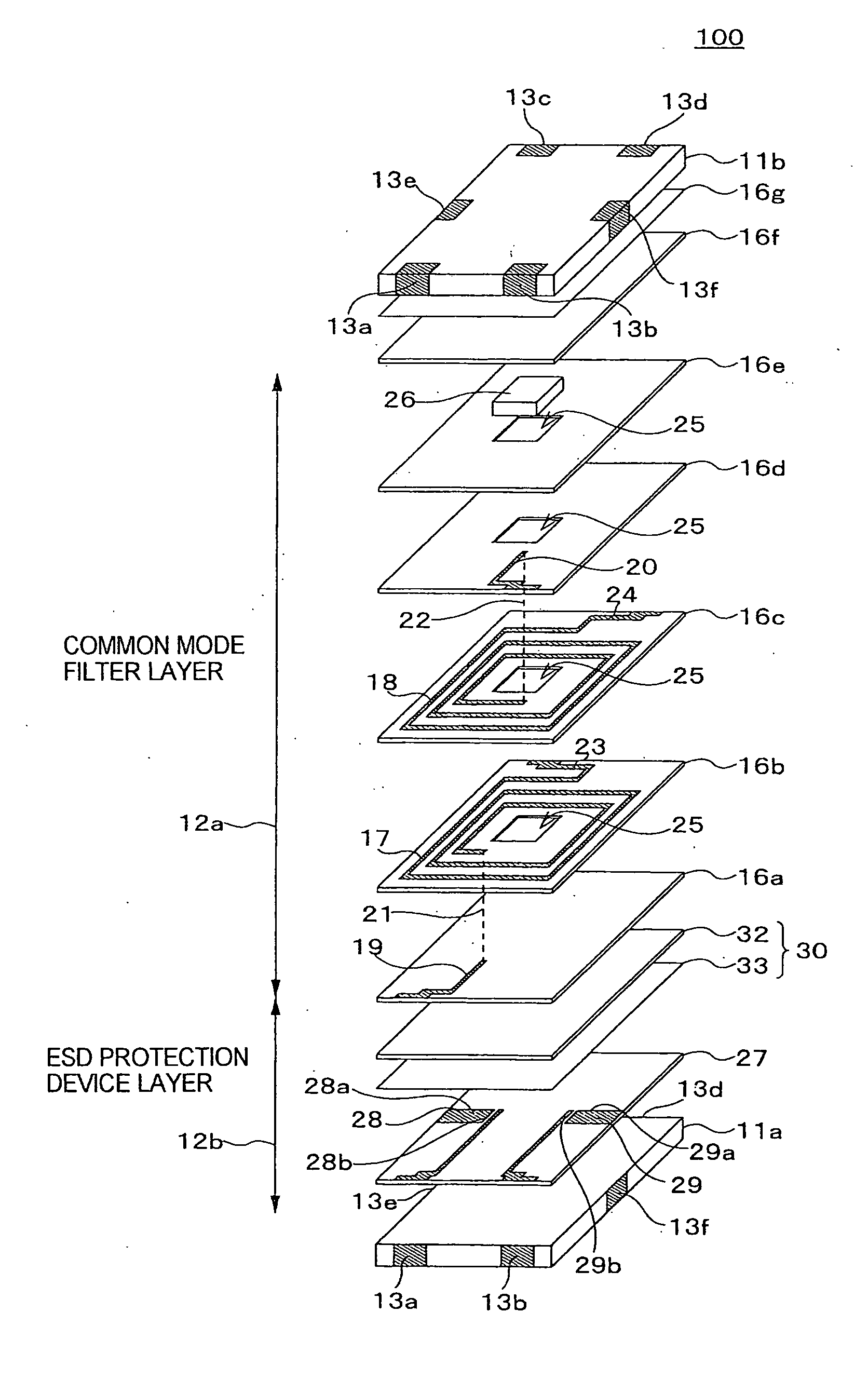
[0066]FIG. 4 is a perspective view schematically showing the external configuration of a preferred embodiment of a composite electronic component according to the present invention.
[0067]As shown in FIG. 4, a composite electronic component 100 according to the present embodiment is a thin-film common mode filter having an electrostatic protection function. The composite electronic component 100 includes a first magnetic base 11a and a second magnetic base 11b, and a composite functional layer 12 sandwiched between the first magnetic base 11a and the second magnetic base 11b. Furthermore, a first terminal electrode 13a to a sixth terminal electrode 13f are formed on the outer peripheral surface of a stack composed of the first magnetic base 11a, the composite functional layer 12, and the second magnetic base 11b. The first and second terminal electrodes 13a and 13b are formed on a first side surface 10a. The third and fourth terminal electrodes 13c and 13d are formed on a second side...
PUM
 Abstract
Description
Claims
Application Information
 - R&D
- Intellectual Property
- Life Sciences
- Materials
- Tech Scout
- Unparalleled Data Quality
- Higher Quality Content
- 60% Fewer Hallucinations
Browse by: Latest US Patents, China's latest patents, Technical Efficacy Thesaurus, Application Domain, Technology Topic, Popular Technical Reports.
© 2025 PatSnap. All rights reserved.Legal|Privacy policy|Modern Slavery Act Transparency Statement|Sitemap|About US| Contact US: help@patsnap.com