Eureka AIR delivers breakthrough ideas for toughest innovation challenges, trusted by R&D personnel around the world.

Image pickup sensor, driving method therefor, and image pickup apparatus

a technology of image pickup and driving method, which is applied in the direction of color television details, television system details, television system deformation, etc., can solve the problems of increased noise voltage, degrading image quality, and affecting the quality of picked-up images, so as to achieve the effect of increasing cos

Inactive Publication Date: 2010-05-27
CANON KK
View PDF4 Cites 17 Cited by
  • Summary
  • Abstract
  • Description
  • Claims
  • Application Information

AI Technical Summary

Benefits of technology

[0038]The present invention provides an image pickup sensor, a driving method therefor, and an image pickup apparatus, which can properly carry out correction processing on noise components at high speed without bringing about an increase in cost.
[0042]According to the present invention, in a case where the noise components of pixel signals of the effective pixel region are corrected for using pixel signals of the plurality of reference pixel regions, it is possible to swiftly carry out correction processing on the noise components without increasing the storage capacity.

Problems solved by technology

However, as the pixel size decreases, the quantity of light incident on each pixel decreases, and therefore, pixels are likely to be affected by noise, bringing about degradation in image quality.
In this case, when the voltage level of the power supply and the GND changes during scanning of one frame, horizontal-striped pattern noise arises in a picked-up image because an amount of change in the voltage level differs according to respective pixel rows.
Namely, the longer the wiring length from the power supply and the GND to a pixel, the greater the wiring impedance on the pixel is, the more greatly the pixel is affected by variations in the voltage level of the power supply and the GND, and the higher the noise voltage is.
However, in a case where reference pixel regions are disposed adjacent to two opposing sides of an effective pixel region, and correction processing is carried out on signals in the reference pixel regions based on correction values calculated in an estimating manner using signals in all the disposed reference pixel regions, the correction processing cannot be efficiently carried out, and the storage capacity of the image processing circuit required for the correction processing must be large in the conventional pixel signal scanning method.
Moreover, the storage capacity of the image processing circuit required for the correction processing has to be such a capacity as to store pixel signals in all the pixels in one row of the effective pixel region and the two reference pixel regions, which requires high cost.

Method used


Image

  • Image pickup sensor, driving method therefor, and image pickup apparatus
  • Image pickup sensor, driving method therefor, and image pickup apparatus
  • Image pickup sensor, driving method therefor, and image pickup apparatus

Examples


first embodiment

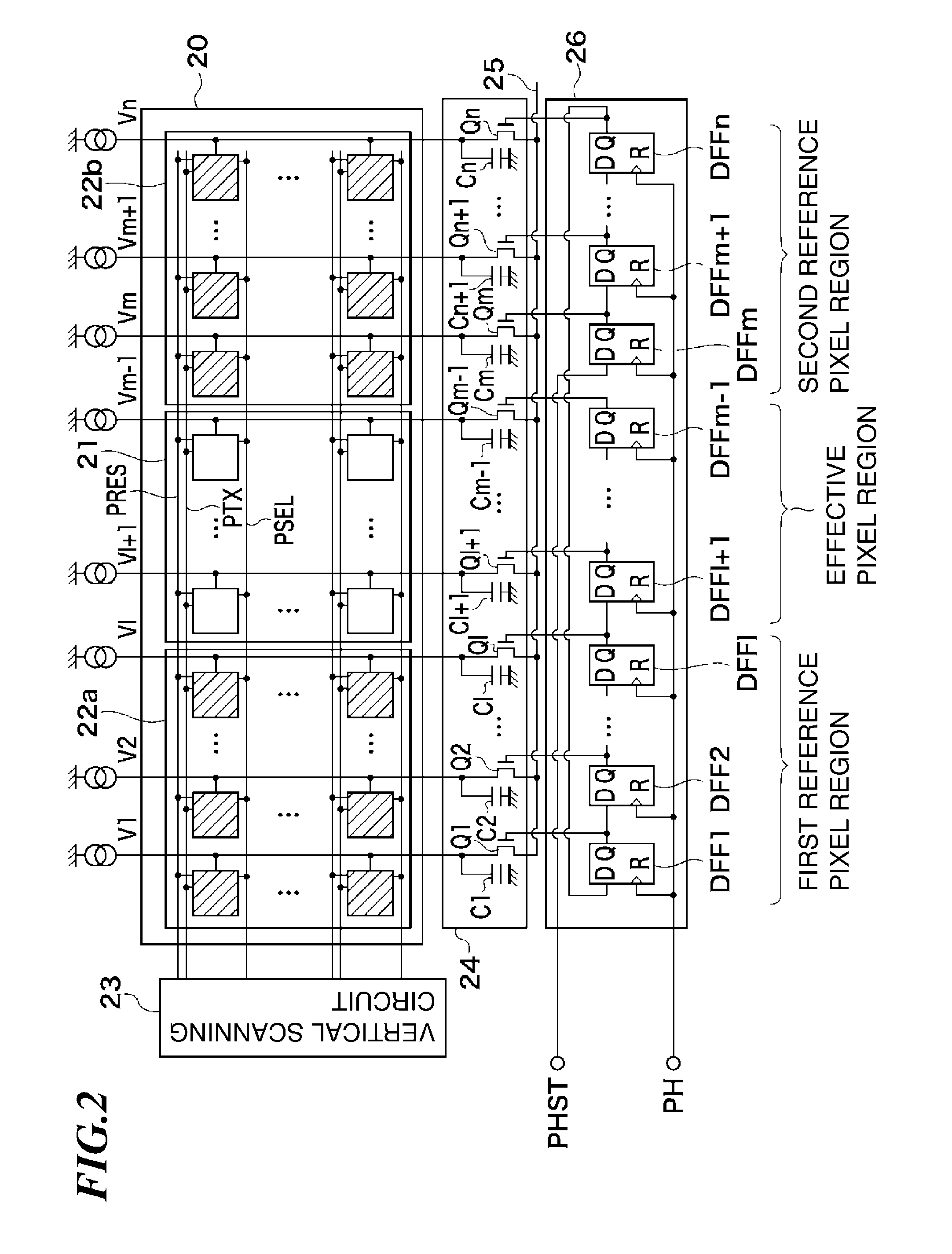
[0087]Referring next to FIG. 3, a detailed description will be given of operation timing of horizontal scanning of pixel signals in the Here, a description will be given mainly of operation timing of horizontal scanning in a pixel array in a pixel row selected for scanning (the same holds for descriptions given by referring to FIGS. 5 and 6).

[0088]The drive circuit 6 causes the vertical scanning circuit 23 to output a vertical scanning pulse signal PV to the pixel unit 20 (t1 to t2). Then, the vertical scanning circuit 23 outputs various control signals as necessary to the respective pixels in the selected row (t2 to t3). As a result, pixel signals of the respective pixels in the selected row are vertically transferred all at once to the line memories C1 to Cn via the vertical output lines V1 to Vn in the respective columns, and held in the line memories C1 to Cn.

[0089]After that, the drive circuit 6 causes the horizontal scanning circuit 26 to input a horizontal scanning start pul...

second embodiment

[0101]Moreover, in the second embodiment, by selectively inputting the horizontal scanning start pulse signal PHST to the signal input terminal (the D input terminal of DFFm) of the second register, the horizontal scanning start position selection unit 47 enables horizontal scanning to be started from the second reference pixel region 22b.

[0102]However, by selectively inputting the horizontal scanning start pulse signal PHST to the signal input terminal (the D input terminal of DFF1) of the first register, the horizontal scanning start position selection unit 47 also enables horizontal scanning to be started from the first reference pixel region 22a.

[0103]It should be noted that three switches 47a, 47b, and 47c included in the horizontal scanning start position selection unit 47 are comprised of NMOS, and turned on when the gate voltage is at H level.

[0104]Thus, when a horizontal scanning start position selection signal STSEL inputted to the horizontal scanning start position sele...

third embodiment

[0122]On the other hand, in the third embodiment, by providing one shift register in the horizontal scanning circuit as in the prior art and carrying out virtual horizontal scanning, horizontal scanning of pixel signals is carried out in the following order: the second reference pixel region 22b→the first reference pixel region 22a→the effective pixel region 21.

[0123]Control of drive for horizontal scanning of pixel signals in the third embodiment is carried out as shown in FIG. 7. In the following description, horizontal scanning of pixel signals in a CMOS sensor (image pickup device 3) arranged as shown in FIG. 10 described above is taken as an example.

[0124]Before starting actual horizontal scanning of pixel signals, the drive circuit 6 inputs a horizontal scanning start pulse signal PHST to a horizontal scanning circuit 1006 (t1 to t3) in a state in which a vertical scanning pulse signal PV has not been inputted to a vertical scanning circuit 1003. Specifically, in the third emb...


PUM


Abstract

An image pickup sensor that can properly carry out correction processing on noise components at high speed without bringing about an increase in cost. In an effective pixel region, pixels for obtaining image pickup signals used as a picked-up image are arranged. A plurality of reference pixel regions in which pixels for obtaining reference signals for the image pickup signals are arranged are disposed adjacent to opposing sides of the effective pixel region. A holding unit holds the image pickup signals obtained from the effective pixel region and the reference signals obtained from the plurality of reference pixel regions, the image pickup signals and the reference signals vertically scanned on a row-by-row basis. A horizontal scanning unit that horizontally scans the image pickup signals and the reference signals held by the holding unit horizontally scans the reference signals held by the holding unit before the image pickup signals.

Description

BACKGROUND OF THE INVENTION[0001]1. Field of the Invention[0002]The present invention relates to an image pickup sensor, a driving method therefor, and an image pickup apparatus.[0003]2. Description of the Related Art[0004]For image pickup apparatuses such as digital cameras and video cameras, a solid-state image pickup device such as a CMOS image sensor is widely used as an image pickup sensor.[0005]In recent years, a solid-state image pickup device has increased in the number of pixels, and the size of each pixel has been made small. However, as the pixel size decreases, the quantity of light incident on each pixel decreases, and therefore, pixels are likely to be affected by noise, bringing about degradation in image quality.[0006]A description will now be given of a principle on which the noise is generated with reference to FIGS. 8 and 9. FIG. 8 is a circuit diagram schematically showing an arrangement of a pixel in a CMOS image sensor (hereinafter referred to as a “CMOS sensor...

Claims


Application Information

Patent Timeline
IPC IPC(8): H04N5/217H04N5/335H04N5/341H04N5/345H04N5/365H04N5/369H04N5/374H04N5/376
CPCH04N5/357H04N5/3765H04N5/361H04N25/60H04N25/63H04N25/745H04N25/40
Inventor YAMAUCHI, MAKIKO
Owner CANON KK
Why Eureka
Eureka Blog
Learn More