
Electronic device and engaging structure thereof

Active Publication Date: 2010-03-11
ASUSTEK COMPUTER INC
View PDF13 Cites 34 Cited by
  • Summary
  • Abstract
  • Description
  • Claims
  • Application Information

AI Technical Summary

Benefits of technology

[0006]Accordingly, an aspect of the present invention is to provide an engaging structure. The engaging structure of the invention applies specific hook and recess to make the assembly comprising the same to be repeatedly disassembled and reassembled with ease.
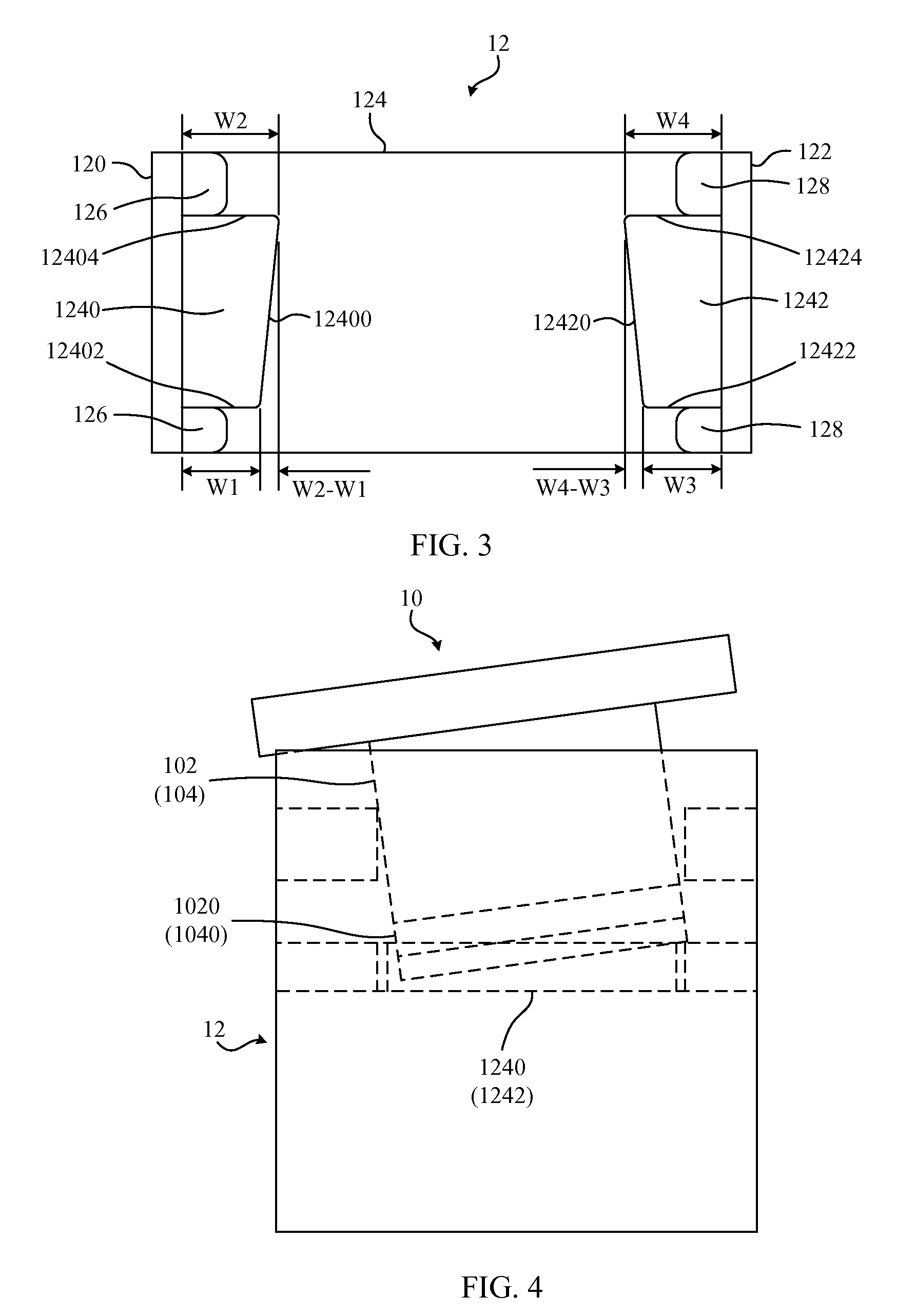
[0011]When the first engaging element and the second engaging element are disassembled, the first rib and the second rib can be applied as a pivot, and the end of the hook can be pulled out from the recess based on the gap. Afterward, the first engaging element can be easily detached from the second engaging element by continuous pulling force.
[0012]Another aspect of the present invention is to provide an electronic device. The electronic device of the invention applied specific hook and recess to make it easier for the casings to be repeatedly disassembled and reassembled. The specific hook and recess are described above. Because there is no need for extra assembly equipments or materials, the present invention can efficiently decrease the cost, labor and time in producing the electronic device.

Problems solved by technology

The trend of the design of the exteriors of electronic devices gets more and more complex.
However, the assembly way (1) adopted will have rubber overflows and bad agglutination occurrence, and after agglutinated, detachment will be impossible; the (2) assembly way make it unable to be detached after assembled, the (3) assembly way uses supersonic wave equipment which is costly, and once there is no way to detach once it is agglutinated.
All in all, most of the tradition ways need to employ extra device or material, which not merely increase the cost of production, but also consume larger amount of manpower in the mean time.

Method used


Image

  • Electronic device and engaging structure thereof
  • Electronic device and engaging structure thereof
  • Electronic device and engaging structure thereof

Examples


Embodiment Construction

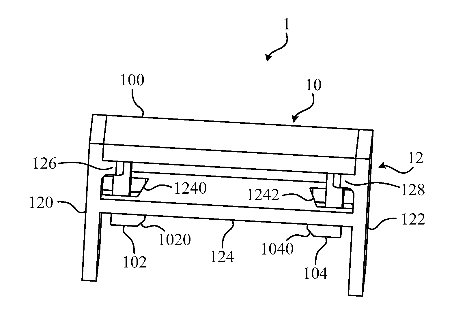
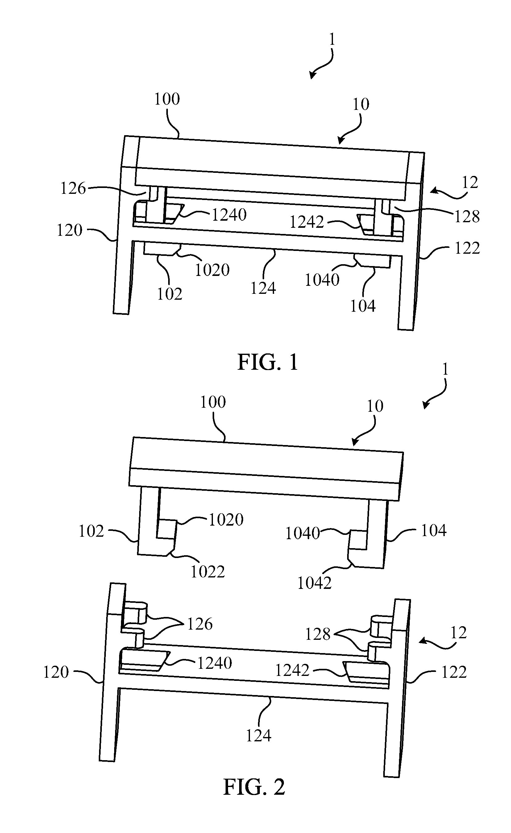
[0024]Please refer to FIG. 1 and FIG. 2. FIG. 1 is a schematic diagram illustrating an engaging structure 1 according to an embodiment of the invention. FIG. 2 is an extendable drawing of the engaging structure 1 of FIG. 1. FIG. 1 is illustrating the engaging structure 1, which is merely something to be described about the technology of the present invention. In other words, the surface of the engaging structure 1 designed should not be confined to the design shown in FIG. 1 it should be applicable in different occasions. The engaging structure 1 can be applied on any electronic device, such as notebook, mobile phone, personal digital assistant (PDA) and electronic dictionary, etc.

[0025]As show in FIG. 1 and FIG. 2. The engaging structure 1 includes the first engaging element 10 and the second engaging element 12. The first engaging element 10 includes the plate portion 100 and two hooks 102 and 104. What must be explained is that the trip quantity may be decided according to the pr...


PUM


Abstract

The invention discloses an electronic device and an engaging structure thereof. The electronic device comprises a first casing and a second casing. The first casing comprises a plate portion and a plurality of hooks. Each hook is located on the plate portion. The second casing comprises a first side portion, a second side portion, an engaging portion, a first rib and a second rib. The engaging portion is between the first and the second side portions and comprises a plurality of recesses. Each recess is engaged with one of the hooks and has a front edge. A gap is between one end of the hook and the front edge of the recess. The first and second ribs are respectively located on the first and the second side portions. The plate portion is disposed on the first and second ribs. The hook can be detached from the recess by the gap.

Description

BACKGROUND OF THE INVENTION[0001]1. Field of the Invention[0002]The present invention relates to an electronic device and an engaging structure thereof, and more particularly, to an engaging structure which can be easily and constantly disassembled and reassembled.[0003]2. Description of the Prior Art[0004]Under the vigorous development of information technology nowadays, more and more functions of electronic devices have been unceasingly developed, such as notebook, mobile phone, personal digital assistant (PDA) and electronic dictionary, etc. They are used in various occasions to meet the demands of the consumers. The trend of the design of the exteriors of electronic devices gets more and more complex. Every device is combined of a lot of electronic elements. In former technology, the following methods were generally selected to carry on the assembly: (1) directly spotting rubber among spare-parts, (2) engaging square recess with general hooks, (3) using supersonic wave.[0005]How...

Claims


Application Information

Patent Timeline
IPC IPC(8): H05K7/00E05C3/04
CPCF16B5/0664G06F1/1656G06F1/1616G06F1/1613Y10T292/1089
Inventor CHEN, CHING CHUNG
Owner ASUSTEK COMPUTER INC
Learn More