
Adhesive tape attaching method

Active Publication Date: 2010-01-07
DISCO CORP
View PDF3 Cites 8 Cited by
  • Summary
  • Abstract
  • Description
  • Claims
  • Application Information

AI Technical Summary

Benefits of technology

[0008]It is therefore an object of the present invention to provide an adhesive tape attaching method which can attach a semiconductor wafer to an adhesive tape without damage to the wafer, wherein a circular recess is formed on the back side of the wafer by grinding only an area corresponding to the device area, and an annular reinforcing portion is formed around the circular recess in an area corresponding the peripheral marginal area surrounding the device area.
[0010]Preferably, the adhesive tape attaching method further includes the steps of supporting the front side of the wafer on an elastic member in the condition where the back side of the wafer is opposed to the adhesive surface of the adhesive tape; and providing an atmospheric-pressure condition in a sealed space formed on the side opposite to a wafer supporting surface of the elastic member, thereby bringing the back side of the wafer into pressure contact with the adhesive surface of the adhesive tape.
[0012]According to the present invention, the plate member is engaged into the circular recess formed on the back side of the wafer by grinding only an area corresponding to the device area formed on the front side of the wafer, thereby attaching the adhesive tape to the back side of the wafer. Accordingly, the wafer can be attached to the adhesive tape without damage to the wafer.

Problems solved by technology

However, such a thin wafer is difficult to handling and there is a possibility of damage to the wafer during transportation thereof.
However, there is a possibility of damage to the thin semiconductor wafer by the pressure of the roller.
However, there arises a problem even when such a device is used to attach the adhesive tape to the semiconductor wafer.
That is, in a semiconductor wafer having a circular recess formed by grinding the back side of the wafer in only an area corresponding to the device area to thereby form an annular reinforcing portion around the circular recess so as to correspond to the peripheral marginal area surrounding the device area, there is a possibility of damage due to the stress generated at the boundary between the annular reinforcing portion and the circular recess in attaching the adhesive tape.

Method used


Image

  • Adhesive tape attaching method
  • Adhesive tape attaching method
  • Adhesive tape attaching method

Examples


Embodiment Construction

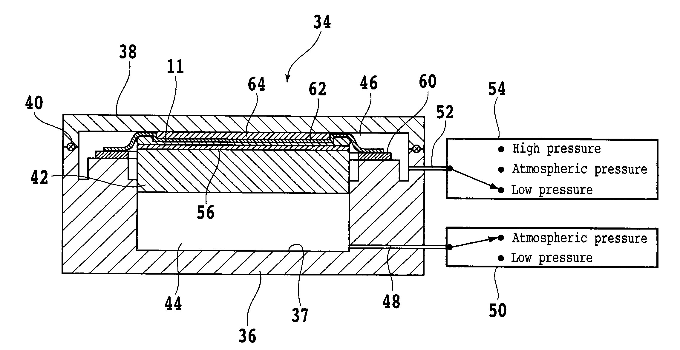
[0022]A preferred embodiment of the present invention will now be described in detail with reference to the drawings. FIG. 1 is a perspective view of a semiconductor wafer 11 before it is processed to have a predetermined thickness. The semiconductor wafer 11 shown in FIG. 1 is a silicon wafer having a thickness of 700 μm, for example. The semiconductor wafer 11 has a front side 11a and a back side 11b. A plurality of crossing streets 13 are formed on the front side 11a of the semiconductor wafer 11 to thereby partition a plurality of rectangular regions where a plurality of devices 15 such as ICs and LSIs are respectively formed.

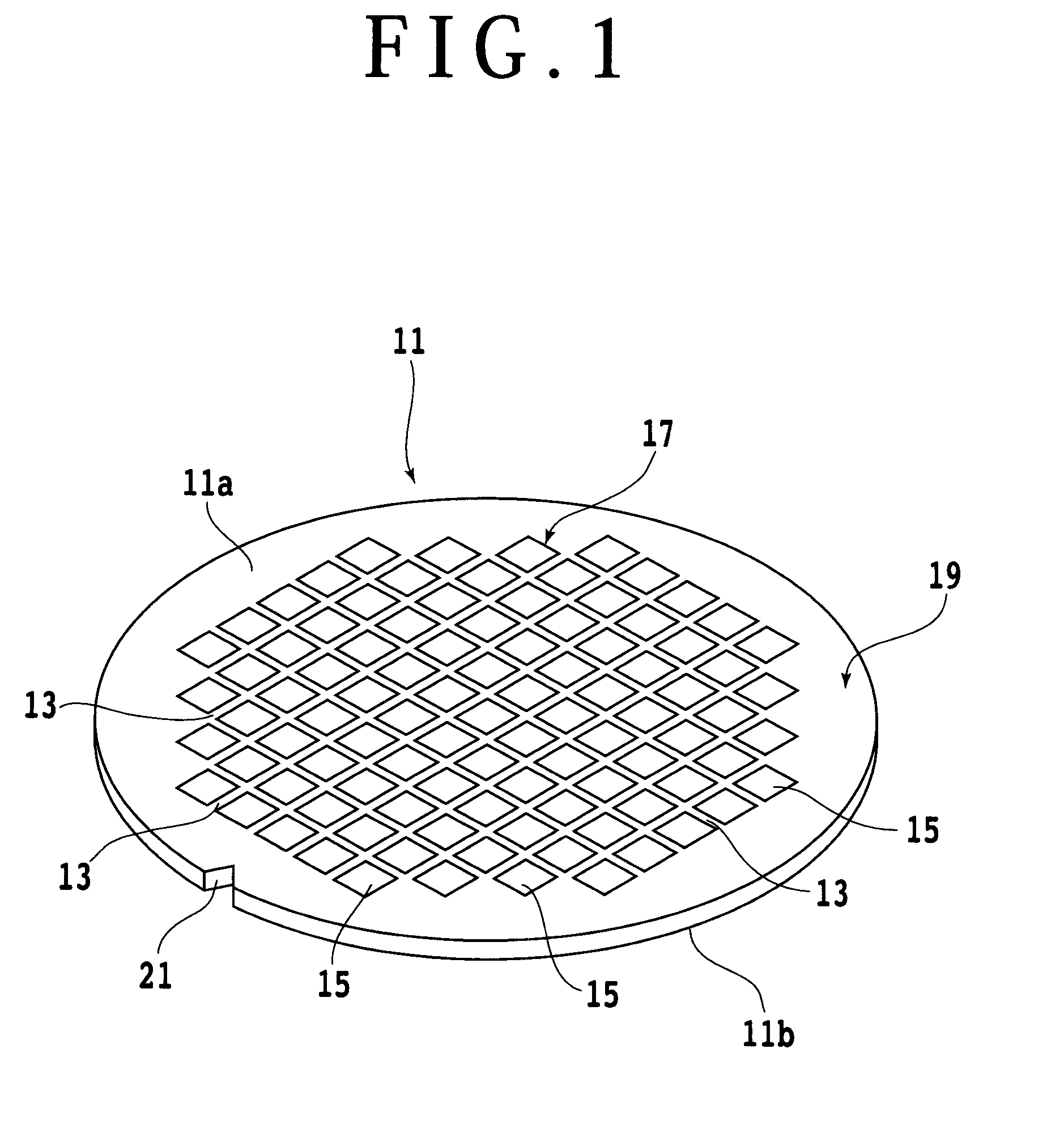
[0023]The semiconductor wafer 11 includes a device area 17 where the devices 15 are formed and a peripheral marginal area 19 surrounding the device area 17. Further, a notch 21 as a mark for indicating the crystal orientation of the silicon wafer is formed on the outer circumference of the semiconductor wafer 11. As shown in FIG. 2, a protective tape 23 is ...


PUM

PropertyMeasurementUnit
Pressureaaaaaaaaaa

Abstract

An adhesive tape attaching method for attaching an adhesive tape to the back side of a wafer, the wafer having a device area where a plurality of devices are formed on the front side of the wafer and a peripheral marginal area surrounding the device area, wherein the back side of the wafer is formed with a circular recess corresponding to the device area and an annular reinforcing portion surrounding the circular recess so as to correspond to the peripheral marginal area. The adhesive tape attaching method includes the steps of holding the wafer and the adhesive tape in a low-pressure condition so that the back side of the wafer is opposed to the adhesive surface of the adhesive tape, fixedly providing a plate member in the condition where the plate member is opposed to the nonadhesive surface of the adhesive tape, pressing the back side of the wafer against the adhesive surface of the adhesive tape, and engaging the plate member into the circular recess formed on the back side of the wafer in the condition where the adhesive tape is closely fitted in the circular recess.

Description

BACKGROUND OF THE INVENTION[0001]1. Field of the Invention[0002]The present invention relates to an adhesive tape attaching method for attaching an adhesive tape to the back side of a wafer having a circular recess on the back side.[0003]2. Description of the Related Art[0004]In a semiconductor device fabrication process, a plurality of crossing division lines called streets are formed on the front side of a substantially disk-shaped semiconductor wafer to thereby partition a plurality of regions where devices such as ICs and LSIs are respectively formed. The semiconductor wafer is cut along these streets by a cutting apparatus to thereby divide the semiconductor wafer into individual semiconductor chips (devices). Prior to cutting the wafer along the streets, the back side of the wafer is ground or polished to reduce the thickness of the wafer to a predetermined value. In recent years, it has been required to further reduce the wafer thickness to about 50 μm, for example, in order ...

Claims


Application Information

Patent Timeline
IPC IPC(8): B32B37/12
CPCH01L21/67132Y10T156/10H01L2221/68327H01L21/6836
Inventor KONDO, AZUMI
Owner DISCO CORP
Learn More