
Photomask data processing method, photomask data processing system and manufacturing method

a technology of photomask data and manufacturing method, which is applied in the field of photomask data processing and photomask manufacturing technique, can solve the problems of significant elongation of the execution time taken by the computer to accomplish correction processing, extended processing time, and frequent disturbance of the regularity of reiterative pattern

Inactive Publication Date: 2009-09-10
FUJITSU SEMICON LTD
View PDF35 Cites 4 Cited by
  • Summary
  • Abstract
  • Description
  • Claims
  • Application Information

AI Technical Summary

Problems solved by technology

However, along with the increasing complexity of processing ensuing from the rising precision of correction processing, the growing fineness of the pattern invites an ever greater scale of pattern data.
This invites a significant elongation of the execution time taken by the computer to accomplish correction processing.
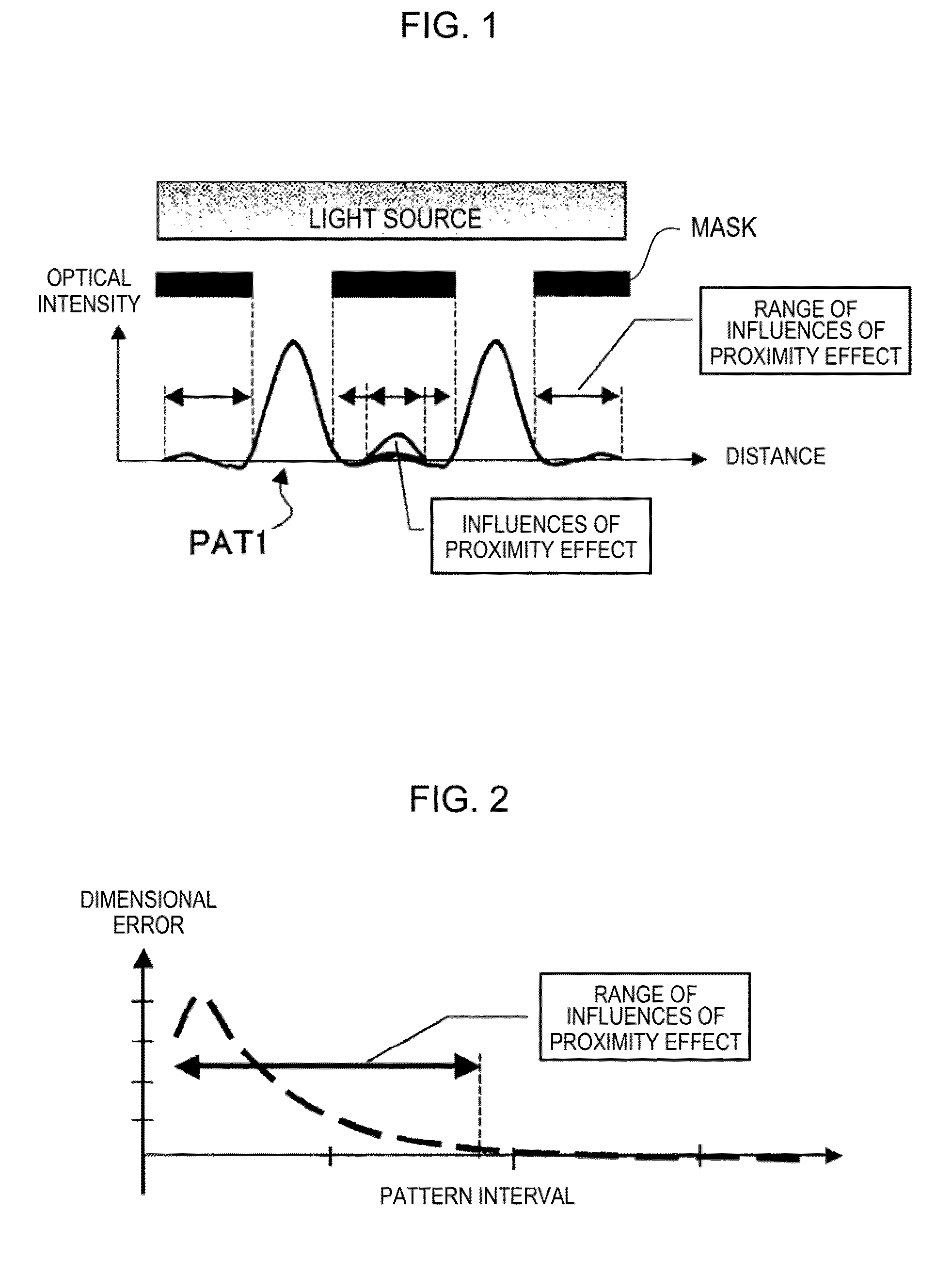
Yet, when correction processing is to be executed by utilizing the hierarchical structure of design data, the regularity of the reiterative pattern is often disturbed by the influence of proximate patterns.
As a consequence, the processing is not completed within the desired time limit, giving rise to a problem of an extended length of time taken by the processing.
However, there is a problem as a matter of real execution that, unless the influences of patterns present around the library pattern are compensated for, no output of normal proximity correction processing can be obtained.
Therefore, this technique can provide no realistic solution.

Method used


Image

  • Photomask data processing method, photomask data processing system and manufacturing method
  • Photomask data processing method, photomask data processing system and manufacturing method
  • Photomask data processing method, photomask data processing system and manufacturing method

Examples


Embodiment Construction

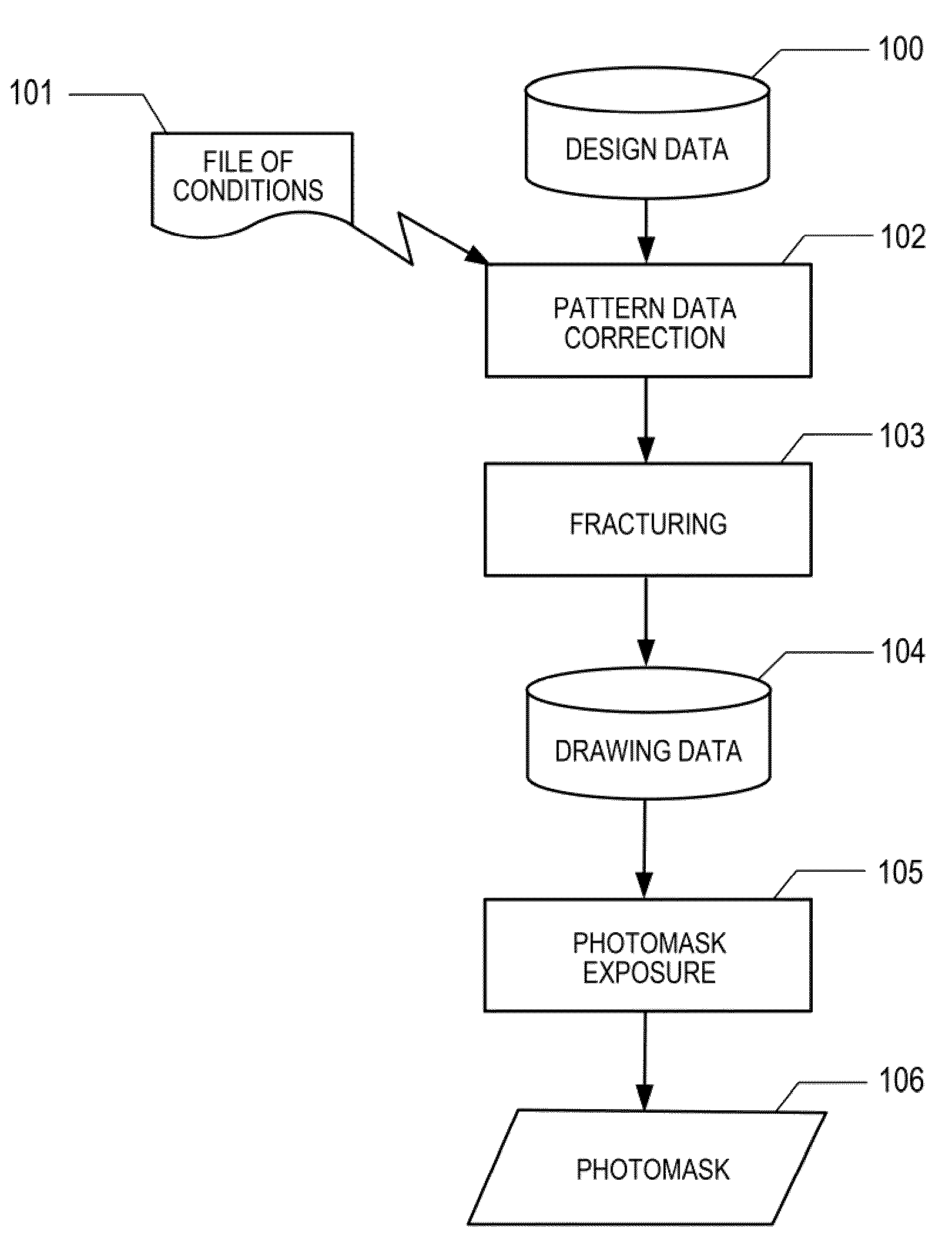
[0028]A pattern data processing system for a semiconductor device, which is an example of an embodiment of the present invention, and a mask manufacturing method using processed pattern data will be described below with reference to accompanying drawings. The configuration of the embodiment is merely an example, and nothing to limit the invention.

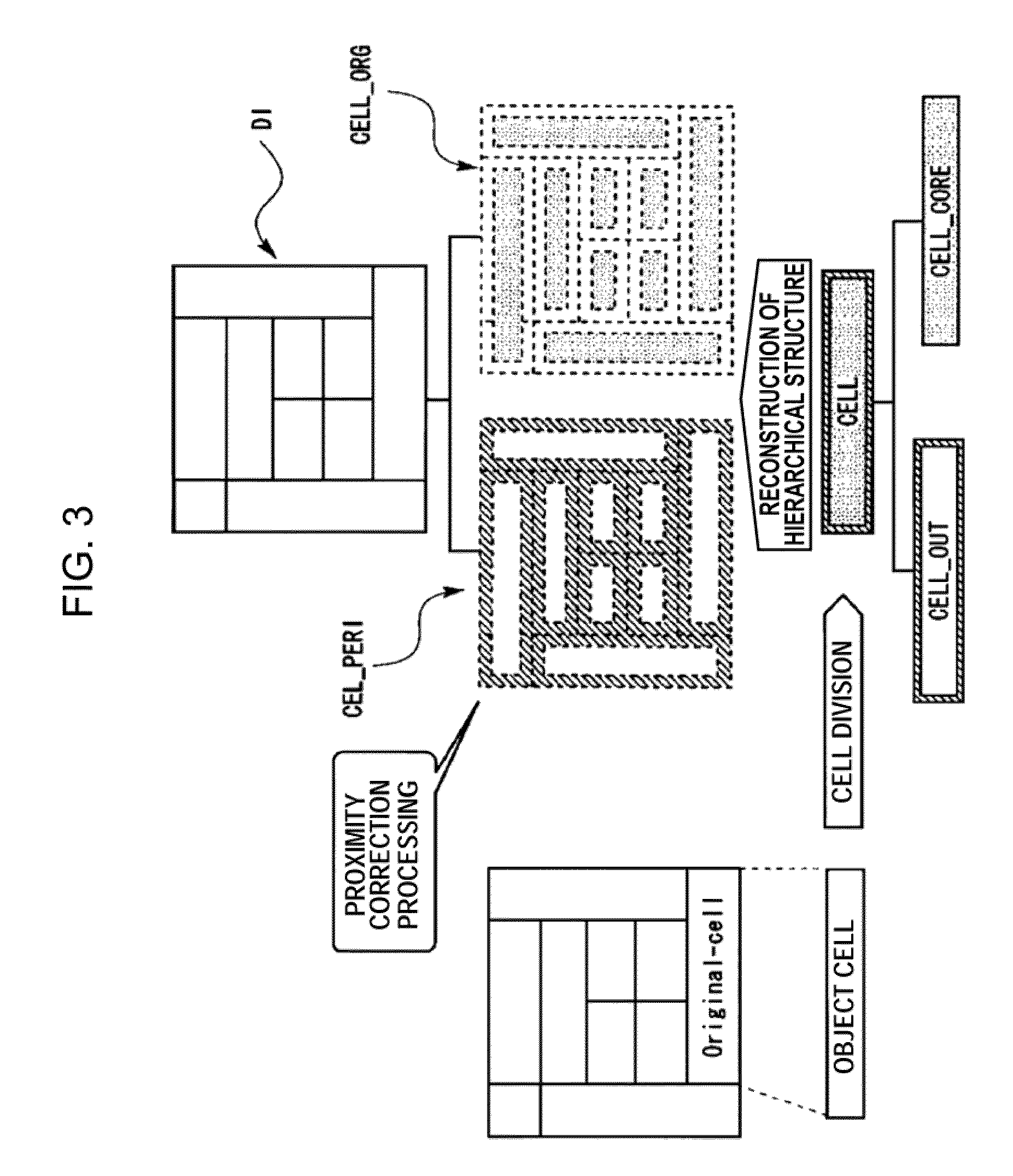
[0029]When design data are to be subjected to optical proximity correction, two methods are available including (1) one which uses the hierarchical structure and (2) the other using a pattern having gone through proximity correction. Each has an effect to shorten the length of time taken to execute correction processing. This embodiment applies these techniques in even more efficient and practically useful ways. For this purpose, this embodiment reconstructs the hierarchical structure of design data and outputs design data permitting easier correction processing. This pattern data processing system has a function to correct optical proximit...


PUM


Abstract

A computer-implemented method, of processing design data to obtain photomask data, includes: selecting, amongst design data, data representing a first cell; selecting a first area in said first cell for which a configuration of a corresponding first pattern is influenced by patterns arranged outward relative to said first cell area; selecting a second area other than said first area in said first cell; constructing a hierarchical structure for said data representing said first cell area that includes said first area and said second area; subjecting the first area to optical proximity correction on the basis of a relationship between the first pattern and the patterns arranged around said first cell area; performing optical proximity correction in said second area on the basis of the first pattern; and synthesizing the corrected first area and the corrected second area, according to the hierarchical structure, to obtain photomask data.

Description

CROSS REFERENCE TO RELATED APPLICATION[0001]This application is based upon and claims the benefit of priority from the prior Japanese Patent Application No. 2008-60118 filed on Mar. 10, 2008, the entire contents of which are incorporated herein by reference.BACKGROUND[0002]1. Field[0003]The present invention relates to a technique for processing photomask data and a photomask manufacturing technique using the same.[0004]2. Description of Related Art[0005]To produce the extremely fine patterns of today's large-scale integrated (LSI) semiconductor circuits, high precision patterning techniques are required. In high precision patterning, processing to correct pattern data, such as optical proximity correction, is applied to design data. Processing to correct pattern data is executed to form the pattern intended to be transferred over a semiconductor substrate from design data. In processing to correct pattern data, the pattern shape of design data is deformed by using a rulebase or opt...

Claims


Application Information

Patent Timeline
IPC IPC(8): G06F17/50G03F1/36G03F1/68G03F1/70H01L21/027
CPCG03F1/36G03F1/144
Inventor OKADA, TOMOYUKI
Owner FUJITSU SEMICON LTD
Learn More