Method for teaching carrier means, storage medium and substrate processing apparatus

a substrate processing and carrier means technology, applied in the direction of electric programme control, instruments, program control, etc., can solve the problems of positional shift, excessive complexity of teaching work, and long time consumption, so as to facilitate teaching work, save time, and improve accuracy

Active Publication Date: 2009-09-03
TOKYO ELECTRON LTD
View PDF5 Cites 9 Cited by
  • Summary
  • Abstract
  • Description
  • Claims
  • Application Information

AI Technical Summary

Benefits of technology

[0027]In the semiconductor processing apparatus according to the present invention, which is configured for carrying the carrier container storing therein a plurality of substrates into the interior of the apparatus, taking out each substrate from the carrier container, then providing a necessary process to the substrates, the jig used for teaching work is held by the carrier means then moved to the preset lowering start position above the table, when the teaching work for the carrier means adapted for carrying the carrier container is performed, for example, upon starting the apparatus. Thereafter, the image of the marker provided to the table and used for detecting the positional shift is taken by the image obtaining means provided to the jig. Subsequently, the correction amount for the lowering start position relative to the ideal position thereof is calculated, based on the result of the step of obtaining the image. Consequently, the lowering start position can be corrected with the correction amount, thereby to obtain the coordinate position of the carrier means on the coordinates of the drive system, corresponding to the ideal position. Thus, the teaching work can be performed automatically, with higher accuracy, without depending on a degree of experience and skill of the operator. In addition, this teaching work can eliminate necessity that the operator should go to each place where the table is provided and do the teaching work for the table, as well as can save time required for the operator to check and obtain the coordinate position, for each table, on the screen. Therefore, this invention can significantly facilitate the teaching work, as such substantially reducing the time required for the work.

Problems solved by technology

Actually, however, because of errors associated with assembling the apparatus and / or errors in the drive system caused, such as by elongation of belts and the like, each constituting the system, the coordinate position of the carrier arm on the design drawing may be somewhat shifted from an ideal position of the carrier arm for a transfer operation.
However, not only upon assembling the apparatus, such a positional shift may also be caused by wear of ball screws and other like parts, due to prolonged continuation of operation of the apparatus.
However, since the operator should do such teaching work in accordance with the manual, the carrier transfer position may include some errors and variations, depending on a degree of experience and skill of the operator and / or by mistakes of the operator upon an input operation or the like.
Therefore, in such a case, the teaching work should be considerably complicated and take much time.
However, neither of these Patent Documents refers to any challenges for addressing the aforementioned problems.

Method used


Image

  • Method for teaching carrier means, storage medium and substrate processing apparatus
  • Method for teaching carrier means, storage medium and substrate processing apparatus
  • Method for teaching carrier means, storage medium and substrate processing apparatus

Examples


Embodiment Construction

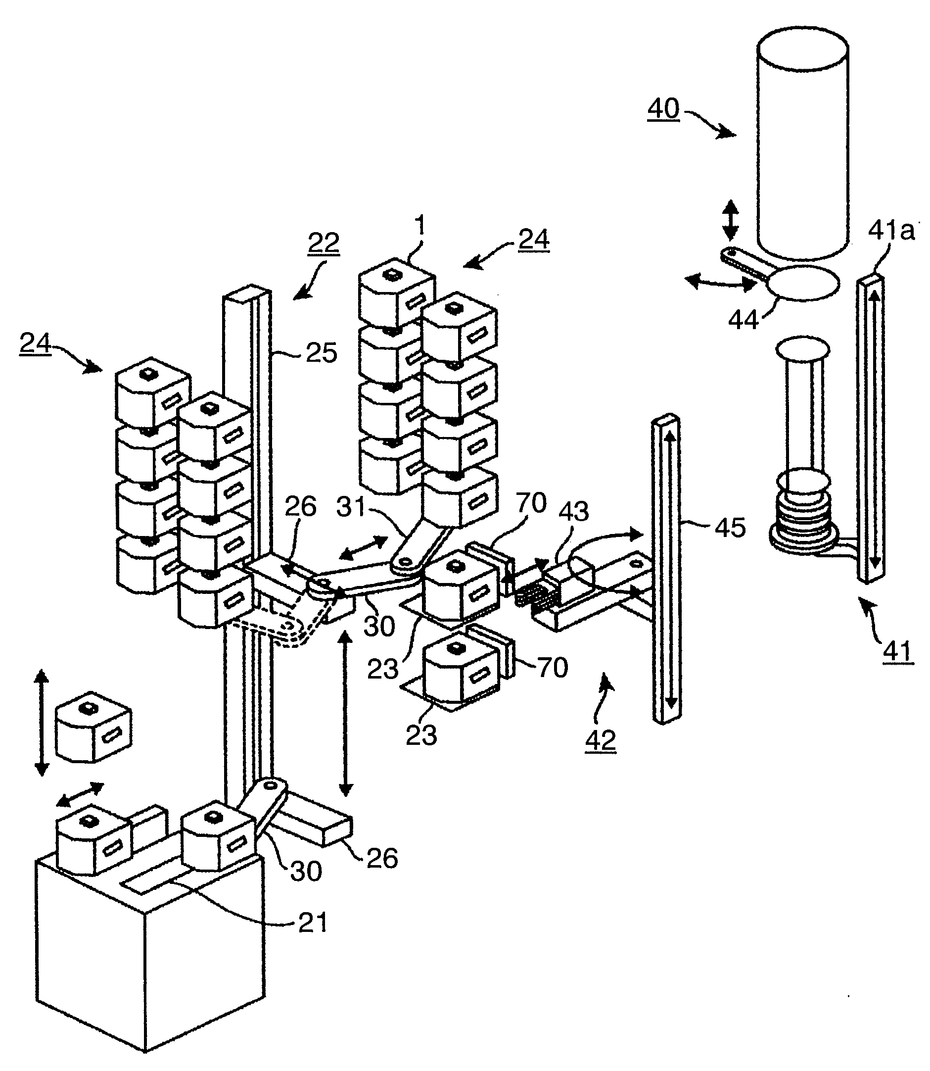
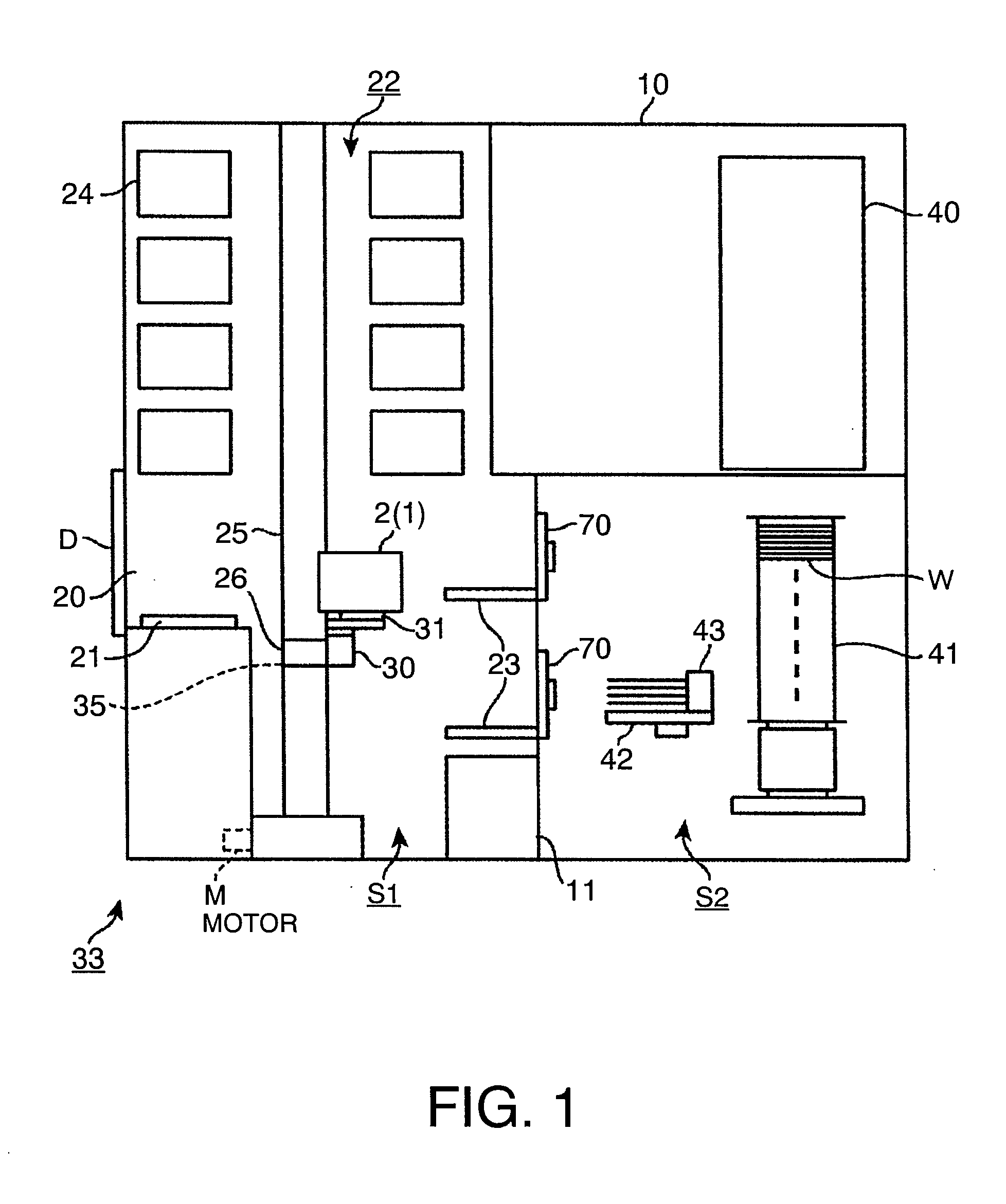
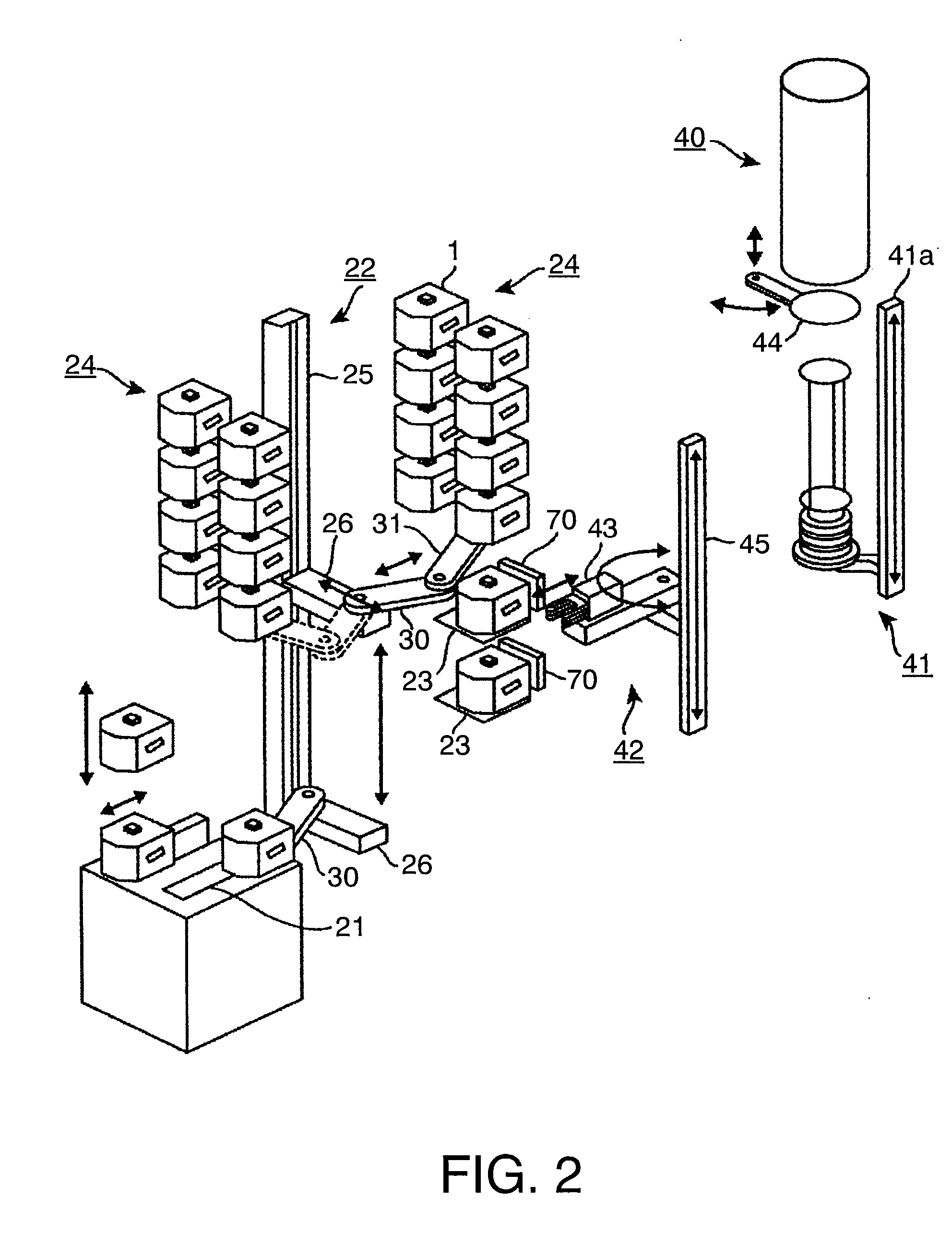
[0040]Hereinafter, one exemplary embodiment of a substrate processing apparatus of the present invention will be described, with reference to FIGS. 1 to 6. In FIG. 1, reference numeral 10 denotes a housing of the substrate processing apparatus. The housing 10 is divided into a working area S1 depicted on the left side and a loading area S2 on the right side, by a partition wall 11. The working area S1 is provided for carrying and storing therein each carrier 1 which is a closed-type carrier container for storing therein multiple sheets (e.g., 25 sheets) of semiconductor wafers (hereinafter referred to as “wafers”). This working area S1 is kept under an ambient atmospheric condition. As shown in the drawing, while a FOUP is used as each closed-type carrier, this is also referred to as the “carrier” herein. In the working area S1, a suitable number of load ports 21, transfer stages 23 and storage units 24 are provided, respectively. Specifically, as shown in FIG. 2, the load ports 21 ...


PUM


Abstract

The present invention is intended to achieve more accurate and facilitated positioning of a carrier onto a table, in a substrate processing apparatus configured for placing the carrier storing multiple sheets of wafers therein, on the table, by using a carrier arm. Before the carrier is actually carried by the carrier arm, a carrier jig having the same shape as the carrier is held by a holding part provided to the carrier arm. The carrier jig is provided with a camera, such that a central position of a region of an image taken by the camera will be coincident with a central position of an opening formed in the table, if the carrier jig is accurately located in an ideal position above the table. First, the carrier arm is actuated to move the holding part of the carrier arm to a preset lowering start position. Then, the image of the region including the opening is taken by the camera. Thereafter, a distance between the central position of the opening and the central position of the region of the image taken by the camera is calculated, so as to obtain an amount of a positional shift, in a horizontal direction, between the preset lowering start position and the ideal position. Consequently, the lowering start position of the holding part is corrected, by using the so-obtained amount of the positional shift as a correction value. Finally, the carrier is placed on the table, based on the so-corrected lowering start position.

Description

CROSS REFERENCE TO RELATED APPLICATIONS[0001]This application is based on the prior Japanese Patent Application No. 2008-050759 filed on Feb. 29, 2008, the entire contents of which are incorporated herein by reference.BACKGROUND OF THE INVENTION[0002]1. Field of the Invention[0003]The present invention relates to a method for teaching a carrier means for carrying a carrier container, in a substrate processing apparatus configured for carrying the carrier container storing therein a plurality of substrates into the interior of the apparatus, taking out each substrate from the carrier container, then providing a process to the substrate. This invention also relates to a storage medium for storing the above method therein, as well as relates to the substrate processing apparatus.[0004]2. Background Art[0005]As one example of semiconductor manufacturing apparatuses, a batch-type vertical substrate processing apparatus configured for providing a heating process, e.g., an oxidizing proces...

Claims


Application Information

Patent Timeline
Patent Type & Authority Applications(United States)
IPC IPC(8): G05B13/02G06F19/00G05B19/04H01L21/68
CPCH01L21/681H01L21/67769G05B19/402G05B2219/45031H01L21/67259H01L21/6773H01L21/67775
Inventor ASAKAWA, TAKASHINAKAMURA, HARUOKIENOMOTO, MASAYUKI
Owner TOKYO ELECTRON LTD
Why Eureka
Try Eureka