Delay locked loop circuit and method for eliminating jitter and offset therein

Active Publication Date: 2009-07-30
HIMAX TECH LTD
View PDF17 Cites 9 Cited by
  • Summary
  • Abstract
  • Description
  • Claims
  • Application Information

AI Technical Summary

Benefits of technology

[0011]In accordance with yet another embodiment of the present invention, a method for eliminating jitter and offset between an input clock signal and an output clock signal in a delay locked loop circuit is provided. The method includes the steps of: determining a phase difference between the input clock signal and a feedback clock signal; generating a difference signal corresponding to the phase difference; sampling the difference signal to output a sampled signal in accordance with the input clock signal; generating a control voltage in accordance with the delay signal; generating a bias voltage corresponding to the control voltage; and delaying the input clock signal in accordance with the bias voltage to generate the output clock signal and the feedback clock signal, wherein the output clock signal has a phase substantially equal to the input clock signal.
[0012]For the foregoing embodiments of the present invention, the delay locked loop (DLL) circuit and the method for eliminating jitter and offset can be applied such that the DLL circuit can operate stably without low pass filter (LPF) and the production cost and size of the DLL circuit can be reduced as well.

Problems solved by technology

However, the operation frequency of the analog DLL circuit 100 described above is still too high, such that the control voltage VCTL changes too fast and the analog DLL circuit 100 cannot work stably.

Method used


Image

  • Delay locked loop circuit and method for eliminating jitter and offset therein
  • Delay locked loop circuit and method for eliminating jitter and offset therein
  • Delay locked loop circuit and method for eliminating jitter and offset therein

Examples


Embodiment Construction

[0019]In the following detailed description, the embodiments of the present invention have been shown and described. As will be realized, the invention is capable of modification in various obvious respects, all without departing from the invention. Accordingly, the drawings and description are to be regarded as illustrative in nature, and not restrictive.

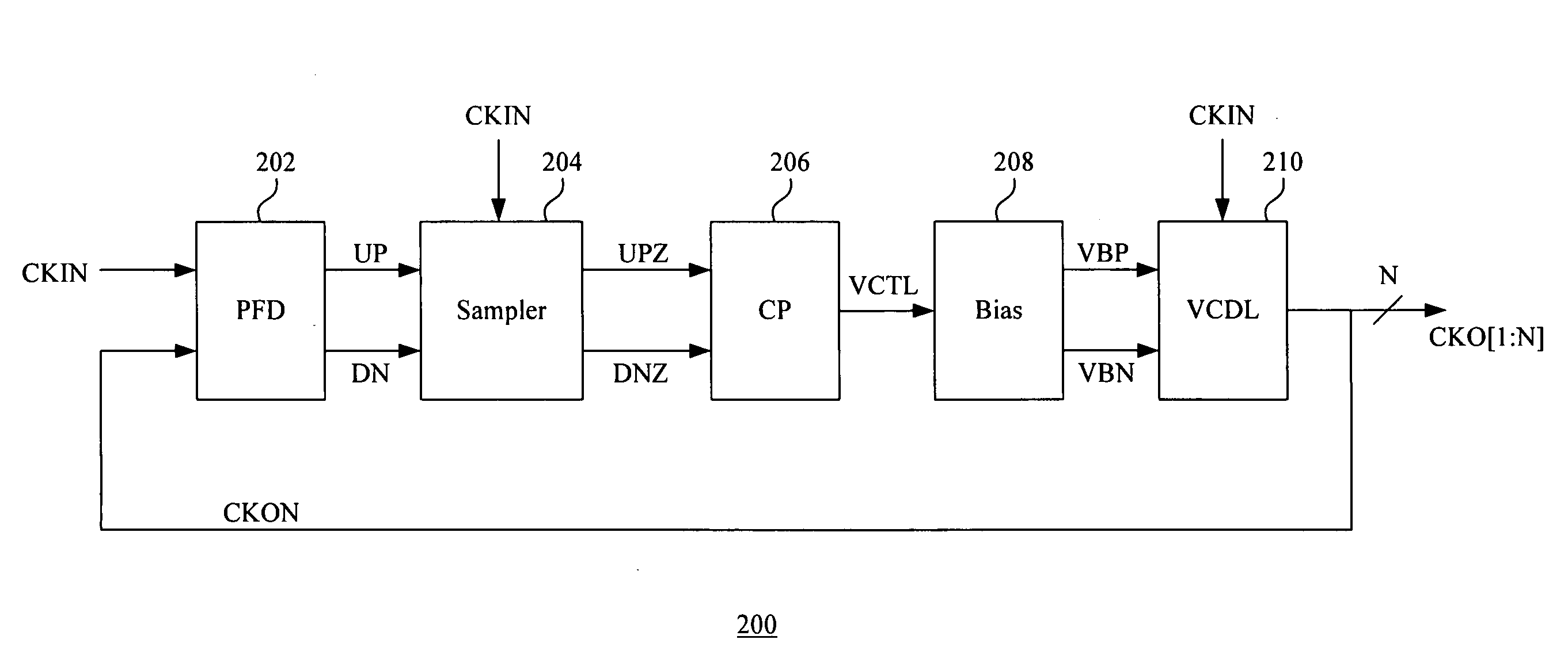
[0020]FIG. 2 illustrates a delay locked loop circuit according to one embodiment of the present invention. The delay locked loop (DLL) circuit 200 includes a phase-frequency detector (PFD) 202, a sampler 204, a charge pump (CP) 206, a bias generator 208 and a voltage-controlled element, e.g. a voltage controlled delay line (VCDL) 210. The phase-frequency detector 202 detects a phase difference between an input clock signal CKIN and a feedback clock signal CKON. The phase-frequency detector 202 has two outputs UP and DN, and outputs at least one difference signal on the UP or DN output after detecting the phase difference between th...


PUM


Abstract

A delay locked loop circuit includes a phase-frequency detector, a sampler, a charge pump, a bias generator and a voltage-controlled element. The phase-frequency detector outputs at least one difference signal by detecting a phase difference between an input clock signal and a feedback clock signal. The sampler outputs at least one sampled signal by delaying the difference signal in accordance with the input clock signal. The charge pump generates a control voltage in accordance with the sampled signal. The bias generator generates at least one bias voltage in accordance with the control voltage. The voltage-controlled element is controlled with the bias voltage to output the feedback clock signal to the phase-frequency detector in accordance with the input clock signal. A method for eliminating jitter and offset between an input clock signal and an output clock signal in a delay locked loop circuit is also disclosed.

Description

BACKGROUND[0001]1. Field of Invention[0002]The present invention relates to a clock synchronization circuit. More particularly, the present invention relates to a delay locked loop (DLL) circuit and a method for eliminating jitter and offset therein.[0003]2. Description of Related Art[0004]Clock synchronization circuits are commonly used in electronic systems to provide good clock distribution, which is very important to overall performance of a product. Examples of such clock synchronization circuits include a phase locked loop (PLL) circuit and a delay locked loop (DLL) circuit. Conceptually, PLL and DLL circuits operate similarly. For DLL circuits, they include analog DLL circuits and digital DLL circuits, in which the analog DLL circuits have different performances from the digital DLL circuits.[0005]FIG. 1 illustrates a typical analog DLL circuit. The analog DLL circuit 100 includes a phase-frequency detector (PFD) 102, a charge pump (CP) 104, a low pass filter (LPF) 106, a bia...

Claims


Application Information

Patent Timeline
IPC IPC(8): H03L7/06
CPCH03L7/0891H03L7/0812H03L7/0816
Inventor HUANG, CHIH-HAUR
Owner HIMAX TECH LTD
Why Eureka
Try Eureka