Method for forming thin film
a thin film and forming technology, applied in the field of fabricating semiconductor devices, can solve the problems of unstable capacitance, hard to secure the required dielectric capacitance, and the limit of the concave type dielectric structure with the stack layer, and achieve the effect of improving the deposition rate of the thin film
- Summary
- Abstract
- Description
- Claims
- Application Information
AI Technical Summary
Benefits of technology
Problems solved by technology
Method used
Image
Examples
first embodiment
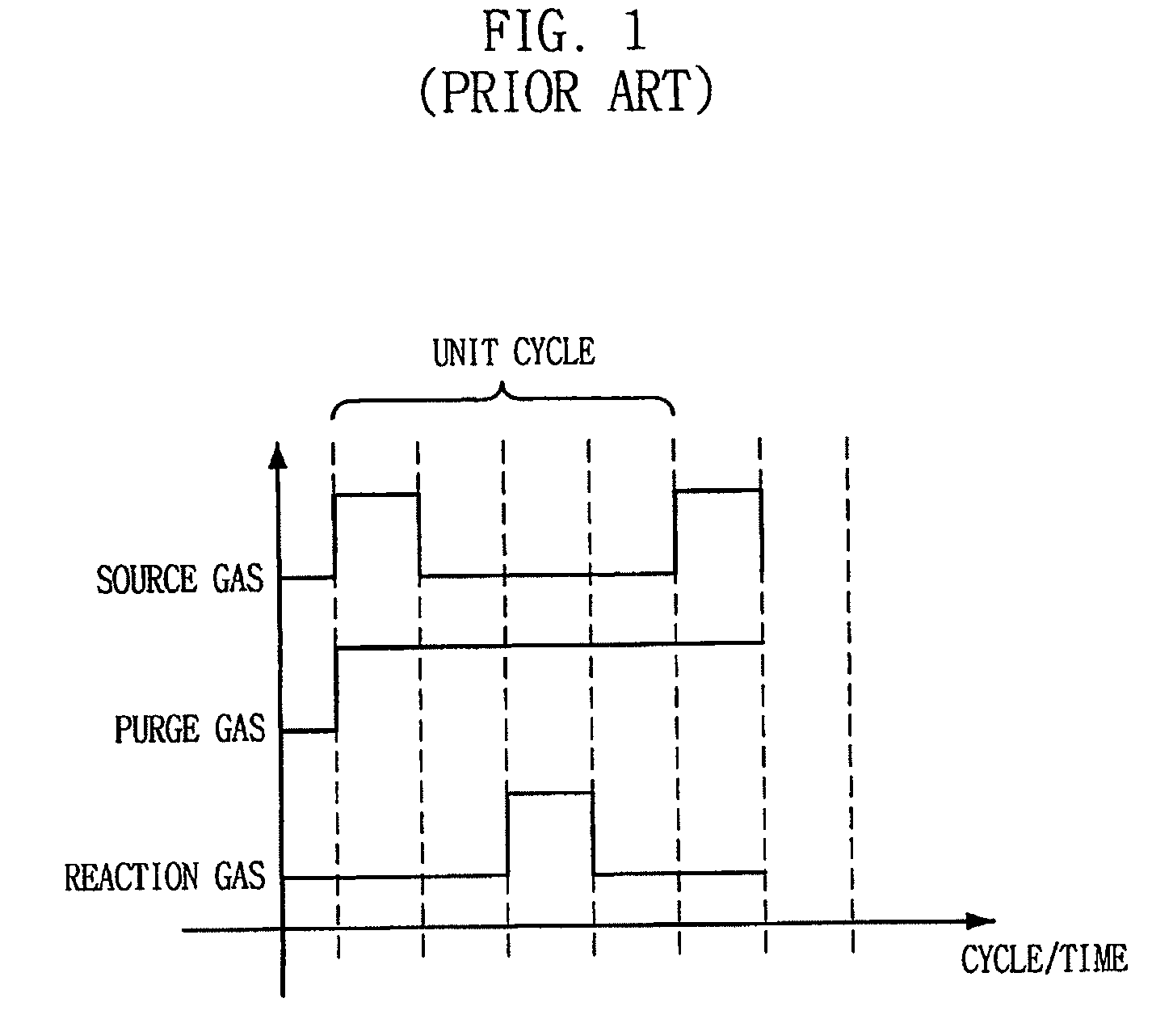
[0042]FIG. 4 is a graph illustrating a specific sequence over time of a method for depositing a thin film in accordance with a first embodiment consistent with the present invention using a cyclic chemical vapor deposition (CVD) method.
[0043]After a wafer is loaded into a chamber, a purge gas, a source gas, and a reaction gas are simultaneously supplied into the chamber. Because the source gas and the reaction gas react with each other almost instantly as they are supplied into the chamber simultaneously, a deposition rate is high.
[0044]Next, while the purge gas continues to be supplied to the chamber, the supply of both the source gas and the reaction gas is discontinued. The purge gas removes, or purges, any remaining reaction byproducts.
[0045]Subsequently, while the purge gas continues to be supplied to the chamber, the reaction gas is simultaneously supplied to the chamber.
[0046]Next, while the purge gas continues to be supplied to the chamber, the supply of the reaction gas is ...
second embodiment
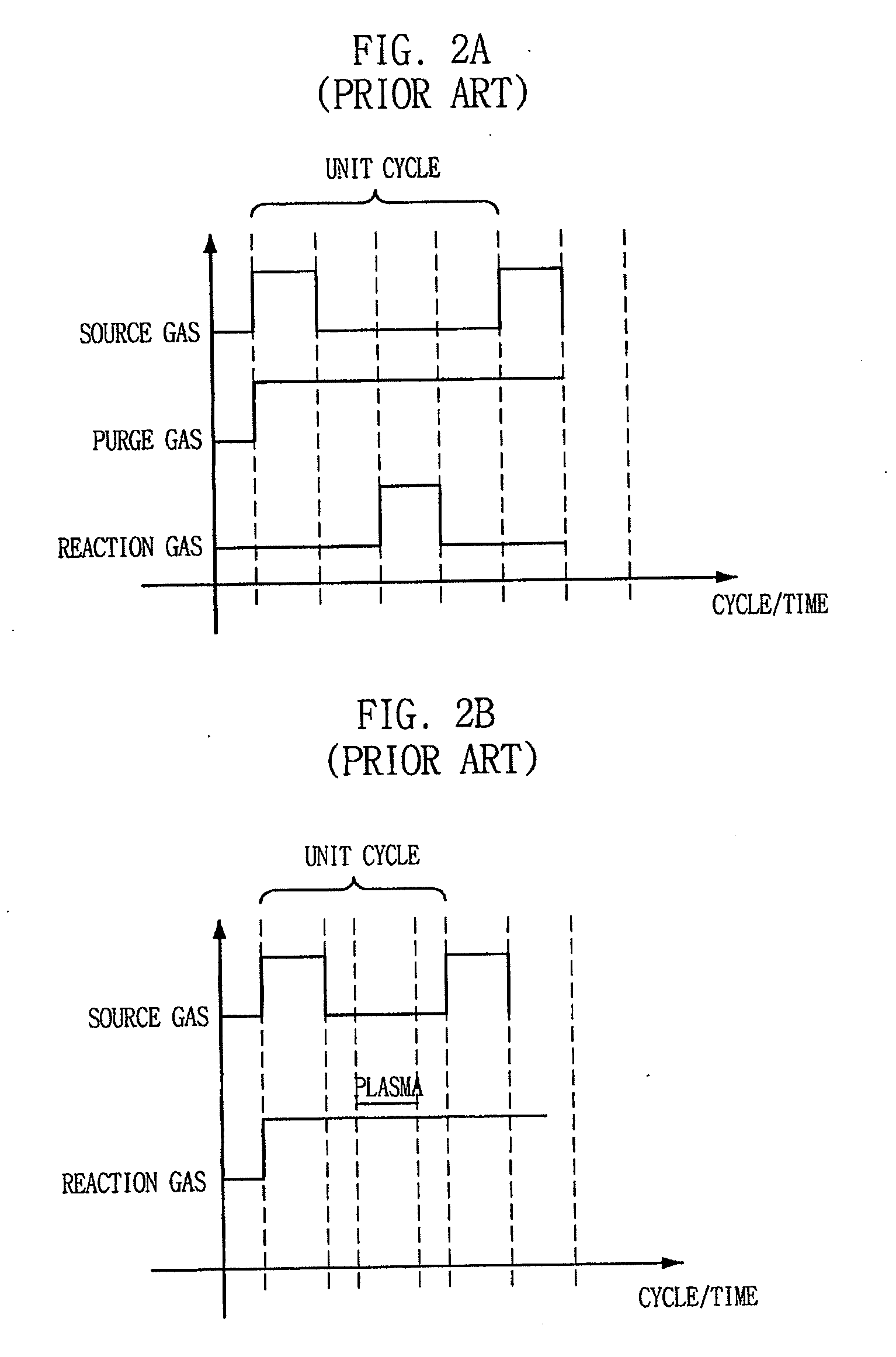
[0047]FIG. 5 is a graph illustrating a specific sequence over time of a method for depositing a thin film in accordance with a second embodiment, which is a modified ALD method.
[0048]Prior to deposition, a wafer is loaded into a chamber. Then, a source gas and a purge gas are simultaneously supplied into the chamber. Next, as the purge gas continues to be supplied into the chamber, the supply of the source gas is discontinued, and the reaction gas is simultaneously supplied into the chamber. When the reaction gas is supplied into the chamber, plasma may be added. Consistent with this embodiment, as shown in FIG. 5, a unit cycle comprises only two steps. Unlike a typical ALD method, additional purge is not performed after the reaction gas is discontinued. additionally performed; however, the purging is continuously performed while a reaction is being performed.
[0049]Because there is reaction gas remaining in the chamber that is not purged, a CVD reaction or a PECVD reaction can occur...
third embodiment
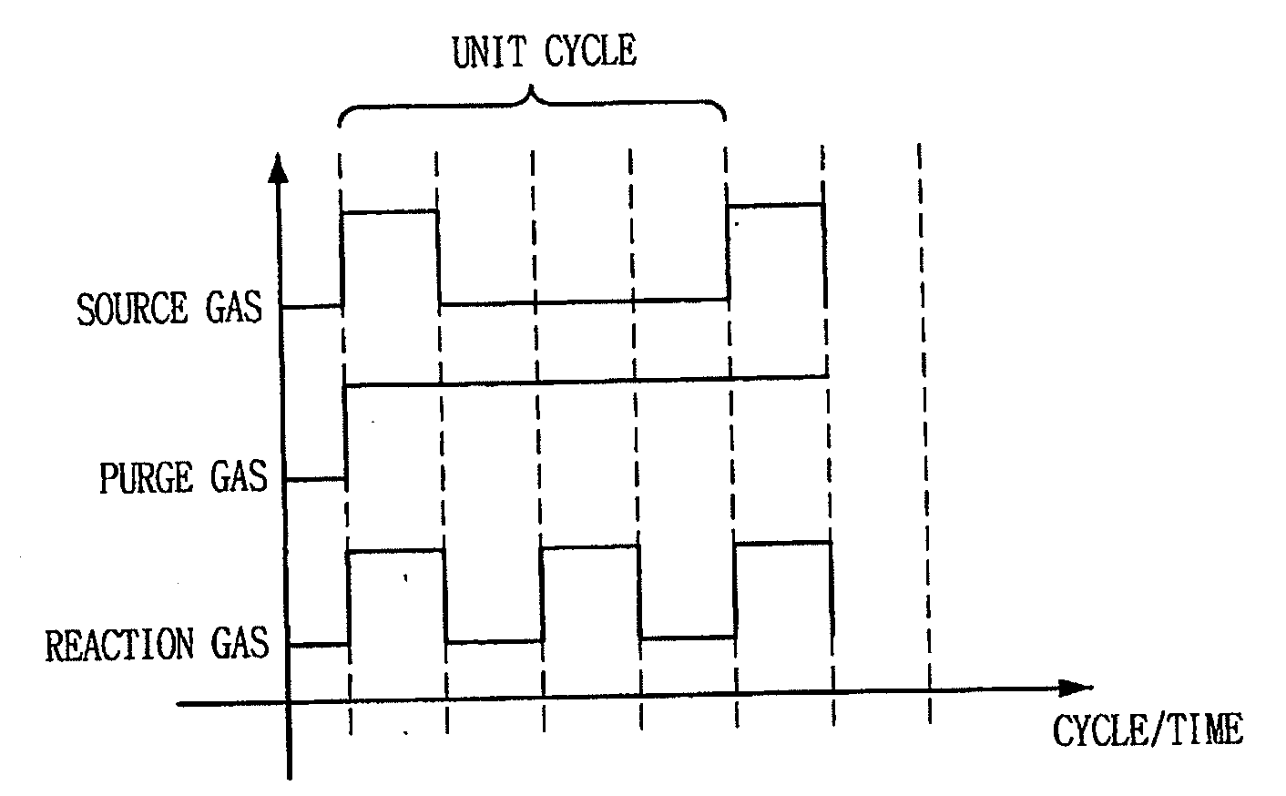
[0050]FIG. 6 is a graph illustrating a specific sequence over time of a method for depositing a thin film in accordance with a third embodiment consistent with the present invention using a cyclic CVD method.
[0051]Prior to deposition, a wafer is loaded into a chamber. Then a reaction gas and a purge gas are continuously supplied into the chamber, and a source gas is periodically supplied into the chamber.
[0052]In this embodiment, a unit cycle comprises a first step of supplying the purge gas, the source gas and the reaction gas simultaneously for a predetermined time and a second step of discontinuing the supply of the source gas.
[0053]A CVD reaction occurs when the source gas and the reaction gas are simultaneously supplied to the chamber. In the absence of the source gas, the thin film is annealed to achieve a higher density and a good quality.
[0054]The unit cycle comprised by the aforementioned steps is repeated until a thin film having a desired thickness is formed.
PUM
| Property | Measurement | Unit |
|---|---|---|
| power | aaaaa | aaaaa |
| power | aaaaa | aaaaa |
| size | aaaaa | aaaaa |
Abstract
Description
Claims
Application Information
 - R&D Engineer
- R&D Manager
- IP Professional
- Industry Leading Data Capabilities
- Powerful AI technology
- Patent DNA Extraction
Browse by: Latest US Patents, China's latest patents, Technical Efficacy Thesaurus, Application Domain, Technology Topic, Popular Technical Reports.
© 2024 PatSnap. All rights reserved.Legal|Privacy policy|Modern Slavery Act Transparency Statement|Sitemap|About US| Contact US: help@patsnap.com


