
Design structure for a high-speed level shifter

a design structure and high-speed technology, applied in logic circuit coupling/interface arrangement, pulse technique, instruments, etc., can solve the problems of large amount of leakage current from the supply rail, and achieve the effect of preventing forward biasing of pn-junction diodes and preventing current leakage from power supplies

Active Publication Date: 2009-06-11
MARVELL ASIA PTE LTD
View PDF5 Cites 0 Cited by
  • Summary
  • Abstract
  • Description
  • Claims
  • Application Information

AI Technical Summary

Benefits of technology

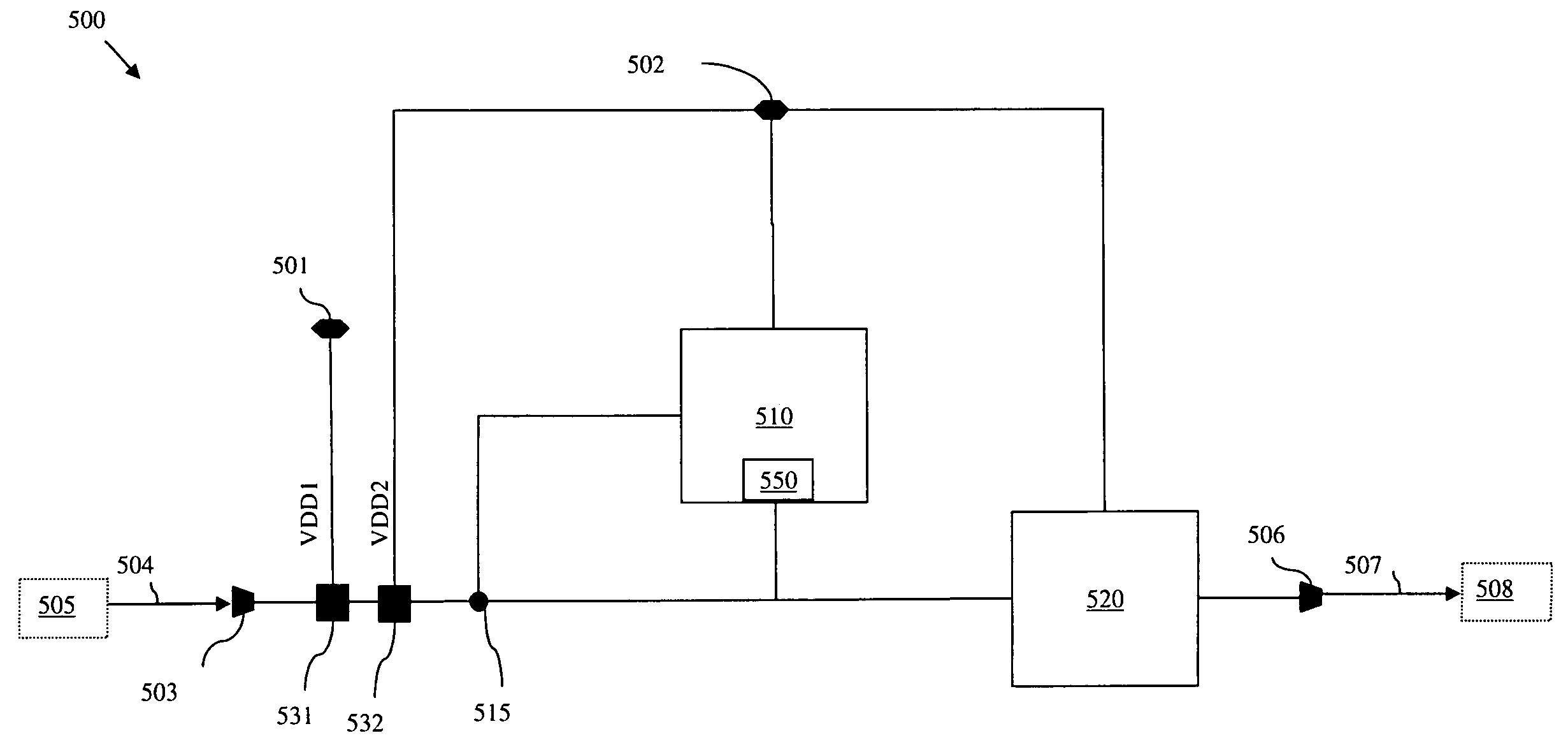
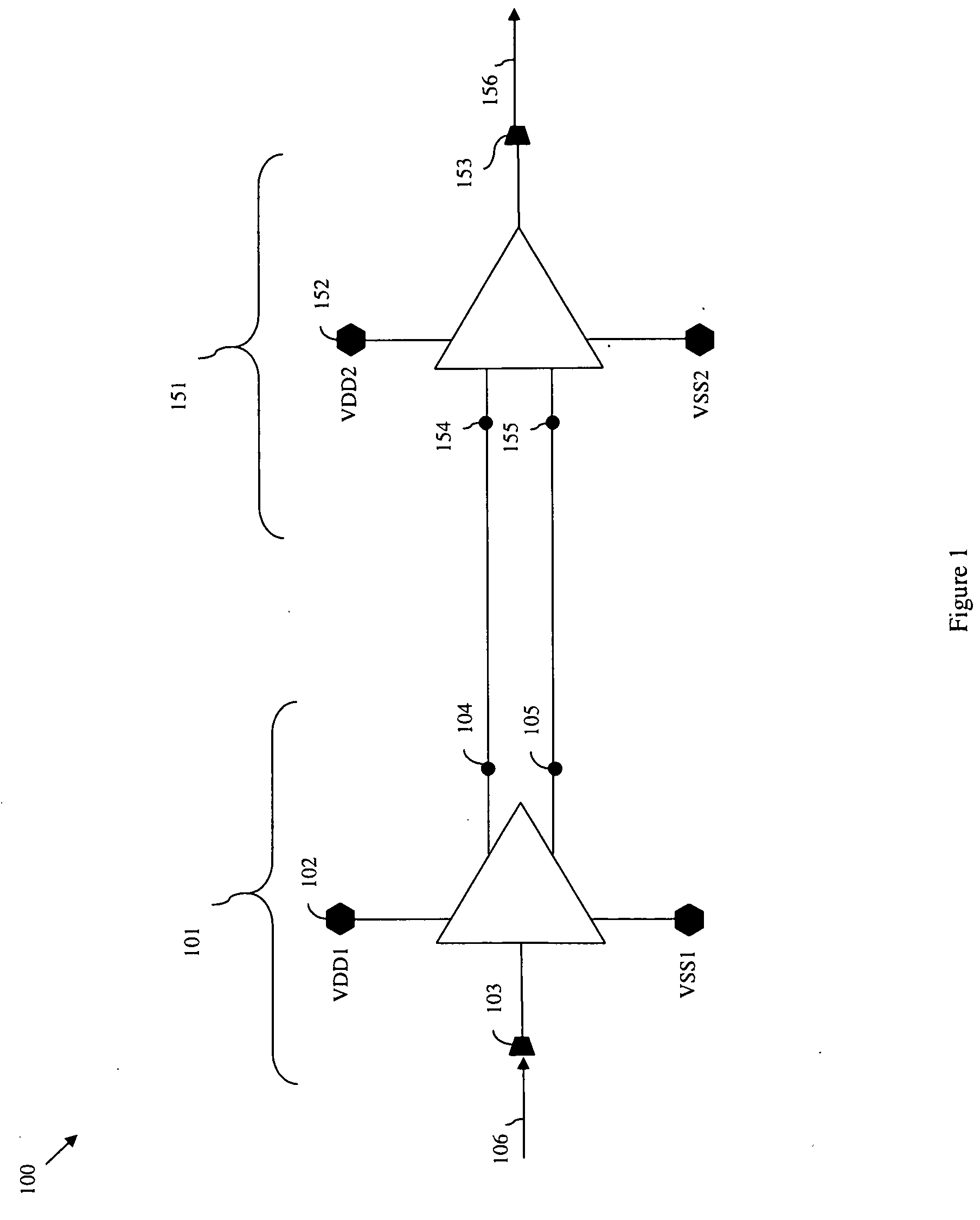
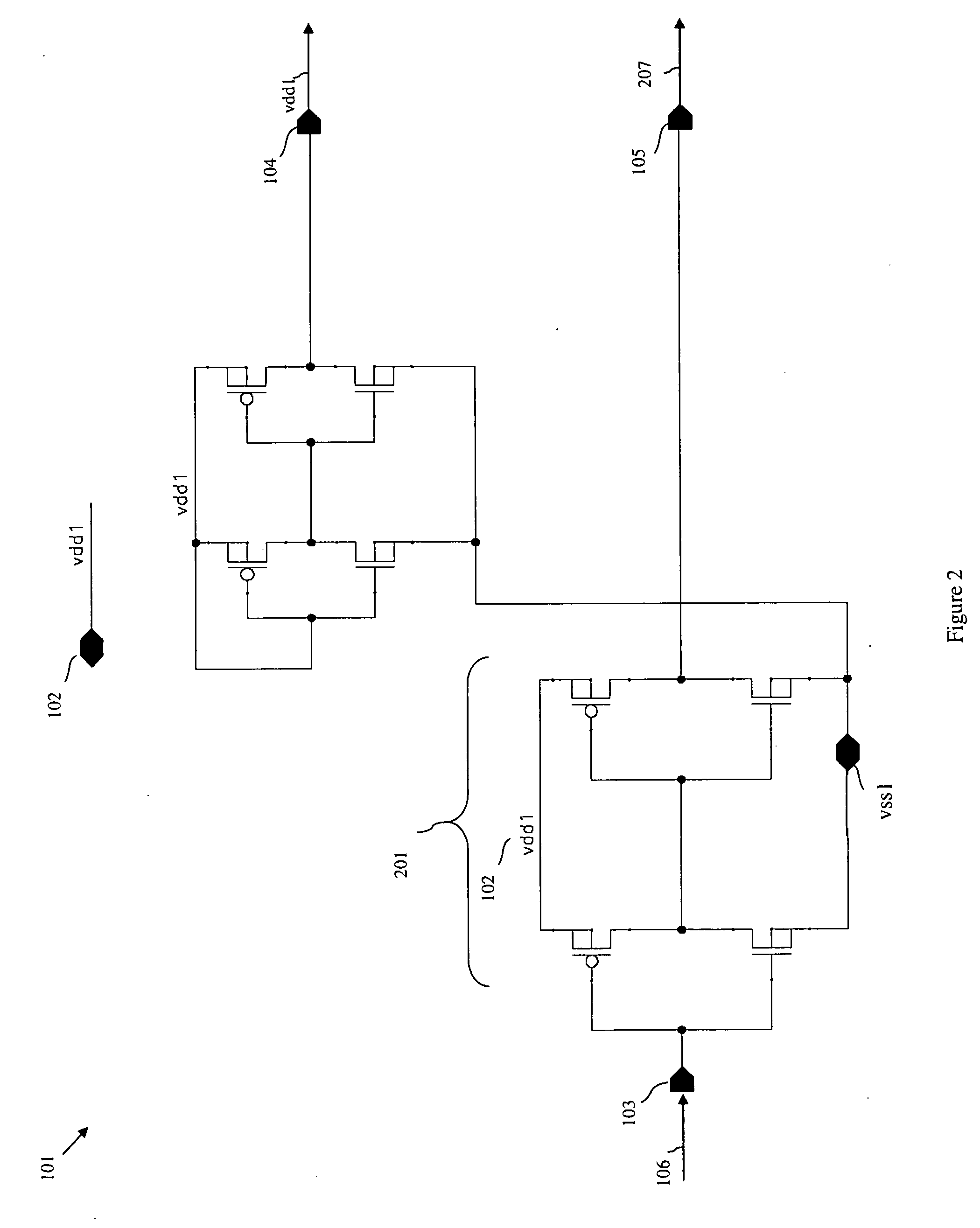
The patent describes a design for a high-speed voltage level shifter circuit that can operate without forming forward biased PN-junction diodes. The circuit includes a pair of series connected switches that are controlled by different power supplies. These switches prevent current leakage from the power supplies and minimize leakage current from power supplies that are not yet powered up. The circuit also includes a voltage adjusting circuit and a buffer circuit to convert signals and pass them on to other devices operating in different voltage domains. The technical effect of this design is to prevent damage to the circuit components and improve the reliability and efficiency of the circuit.

Problems solved by technology

However, due to asynchronous power-up sequences, high speed voltage level shifter circuits have a tendency to suffer from large amounts of leakage current from the supply rails.

Method used


Image

  • Design structure for a high-speed level shifter
  • Design structure for a high-speed level shifter
  • Design structure for a high-speed level shifter

Examples


Embodiment Construction

[0033]The embodiments of the invention and the various features and advantageous details thereof are explained more fully with reference to the non-limiting embodiments that are illustrated in the accompanying drawings and detailed in the following description. It should be noted that the features illustrated in the drawings are not necessarily drawn to scale. Descriptions of well-known components and processing techniques are omitted so as to not unnecessarily obscure the embodiments of the invention. The examples used herein are intended merely to facilitate an understanding of ways in which the embodiments of the invention may be practiced and to further enable those of skill in the art to practice the embodiments of the invention. Accordingly, the examples should not be construed as limiting the scope of the embodiments of the invention.

[0034]Disclosed herein are embodiments of a design structure for a high speed voltage level shifter circuit capable of translating voltage level...


PUM


Abstract

Disclosed are embodiments of a design structure for a voltage level shifter circuit that operates without forward biasing junction diodes, regardless of the sequence in which different power supplies are powered up. The circuit embodiments incorporate a pair of series connected switches (e.g., transistors) between an input terminal and a voltage adjusting circuit. Each switch is controlled by a different supply voltage from a different power supply. Only when both power supplies are powered-up and the different supply voltages are received at both switches will a first signal generated using one of the supply voltages be passed to a voltage adjusting circuit and thereafter converted into a second signal representative of the first signal, but generated using the second supply voltage. Incorporation of the pair of series connected switches into the voltage level shifter circuit prevents forward biasing of junction diodes in the circuit and thereby prevents current leakage from the power supplies.

Description

CROSS-REFERENCE TO RELATED APPLICATIONS[0001]This application is a Continuation of U.S. application Ser. No. 11 / 869,146 filed Oct. 9, 2007, the complete disclosure of which, in its entirety, is herein incorporated by reference.BACKGROUND[0002]1. Field of the Invention[0003]The embodiments of the invention generally relate to voltage level shifters and, more particularly, to a design structure for high-speed voltage level shifter circuit with no power-on sequencing requirement as well as a design structure on which the circuit resides.[0004]2. Description of the Related Art[0005]Voltage level shifter circuits are widely used in analog and mixed signal designs having multiple voltage domains. Such voltage level shifter circuits convert signals from one voltage level domain to another. For example, a voltage level shifter circuit can be designed to convert a signal from a device operating under a first power supply, which provides a first supply voltage VDD1, so that it can be processe...

Claims


Application Information

Patent Timeline
Patent Type & Authority Applications(United States)
IPC IPC(8): H02J1/00G06F17/50
CPCH03K19/018521
Inventor BANERJEE, ANIRBANGEISSLER, STEPHEN F.HO, SHIU CHUNG
Owner MARVELL ASIA PTE LTD
Learn More