
Semiconductor optical amplifier

Active Publication Date: 2009-05-14
FUJITSU LTD
View PDF9 Cites 8 Cited by
  • Summary
  • Abstract
  • Description
  • Claims
  • Application Information

AI Technical Summary

Benefits of technology

[0015]According to an aspect of the invention, a semiconductor optical amplifier includes: a semiconductor substrate; and an active layer provided above the semiconductor substrate, the amplifier amplifying an incident signal light incident on a light incident end surface by suppressing resonance of light due to reflection on the light incident end surface and on a light emission end surface of the active

Problems solved by technology

The SOA also needs to be used in a linear region with the saturation optical output power being sufficiently increased because it causes, when used in a saturation region, a transmission penalty due to deterioration in waveform and crosstalk between wavelength channels caused by the pattern effect.
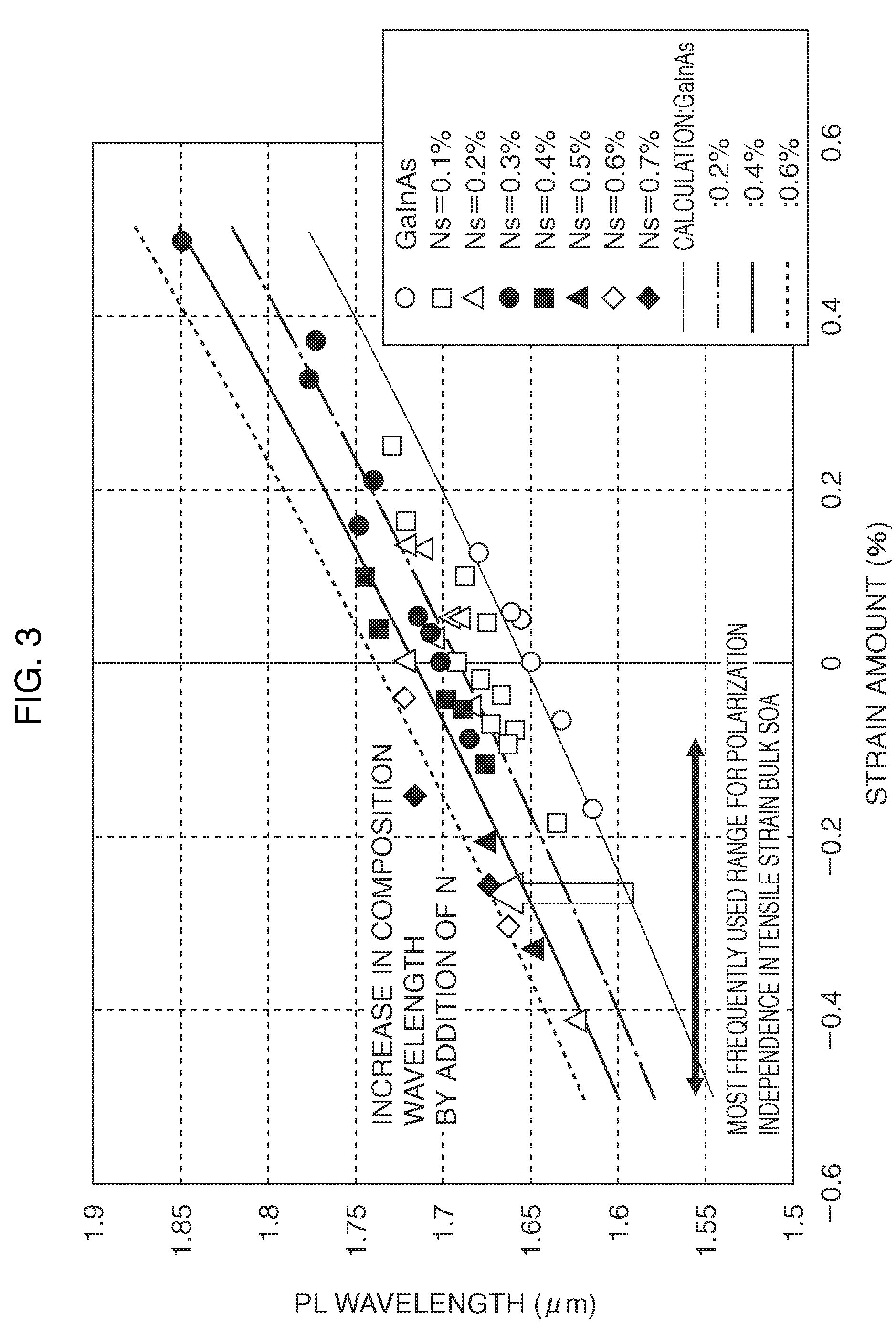
In this SOA, however, the introduction of the tensile strain into the active layer can suppress the polarization dependent gain to low but brings about a problem of the gain peak wavelength reducing in wavelength.
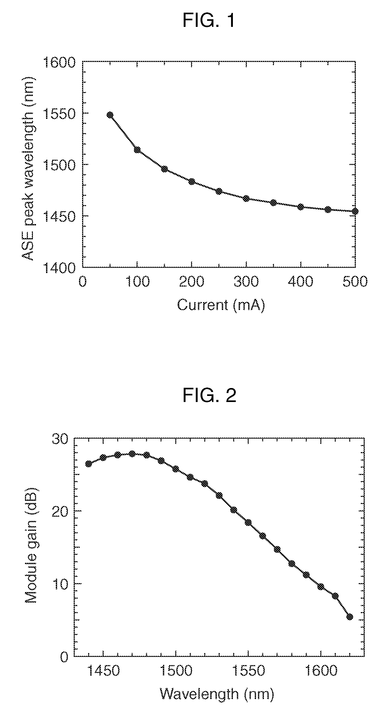
Thus, a problem is to satisfy both polarization independence and high saturation optical output power of the SOA as well as to obtain a high gain in C-band and L-band used in an optical fiber communication system, especially in L-band.

Method used


Image

  • Semiconductor optical amplifier
  • Semiconductor optical amplifier
  • Semiconductor optical amplifier

Examples


Embodiment Construction

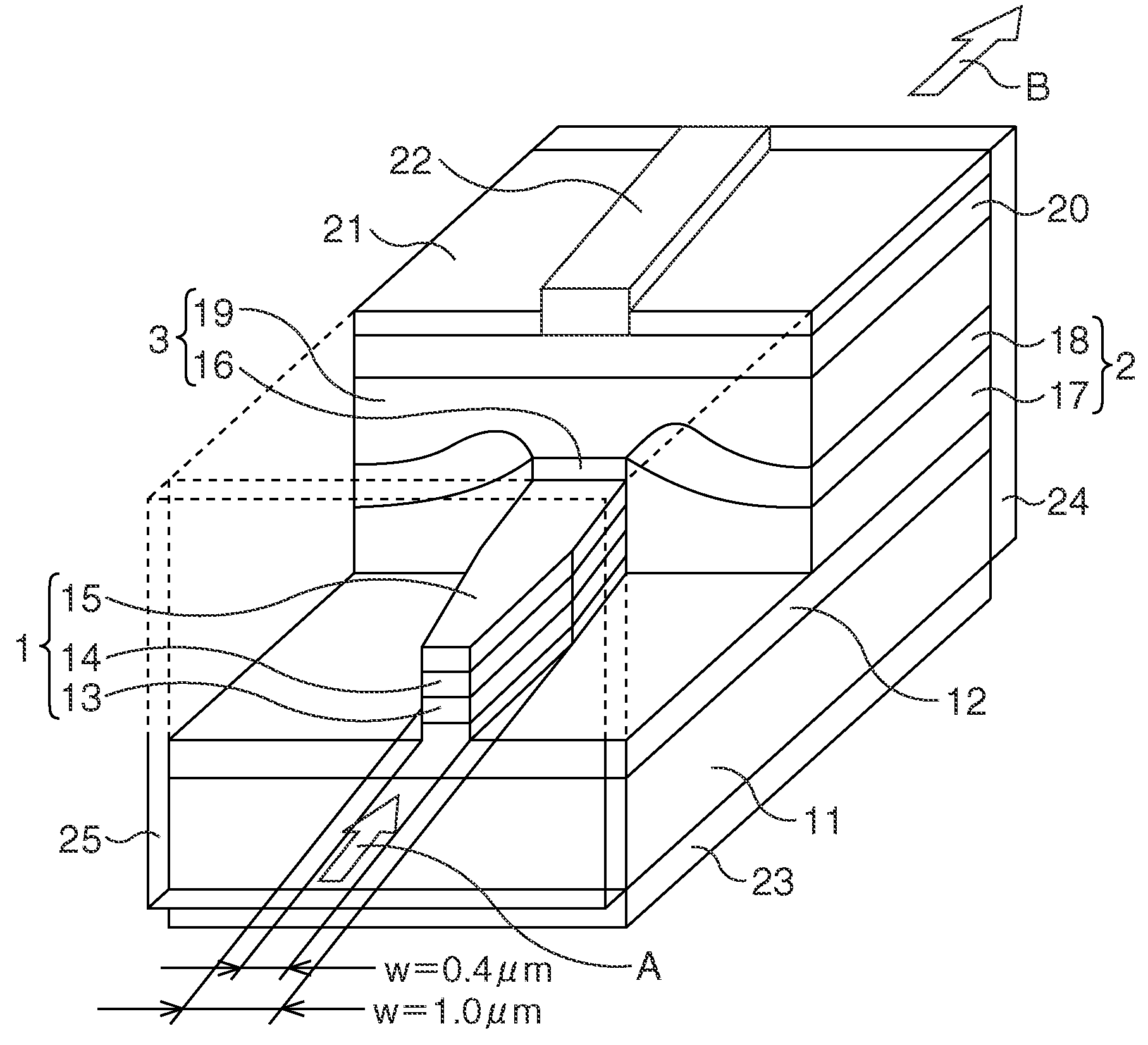
[0023]The present invention provides a polarization-independent SOA using an InP substrate as a semiconductor substrate and using GaInNAs having introduced tensile strain as an active layer.

[0024]With the above-described configuration, the polarization independence is achieved by introducing the tensile strain, and the high saturation optical output power is realized by reducing the film thickness of the active layer as well as the gain peak wavelength is increased by reducing the band gap of the active layer through use of GaInNAs made by adding nitrogen (N) to GaInAs as a material of the active layer so as to achieve high gain especially in C-band and L-band even when band filling exits at the time of injecting a high current into the active layer.

[0025]As described above, since the flatness of the active layer cross section is high in the SOA with high saturation optical output power, a light confinement factor (ΓTE) to the polarized light in the TE mode (TE polarized light) is l...


PUM


Abstract

A polarization-independent SOA is provided which uses an InP substrate (11) as a semiconductor substrate and uses GaInNAs having introduced tensile strain as an active layer (14). With this configuration, the polarization independence is achieved by introducing the tensile strain, and high saturation optical output power is realized by reducing the film thickness of the active layer (14) as well as the gain peak wavelength is increased by reducing the band gap of the active layer (14) through use of GaInNAs made by adding nitrogen (N) to GaInAs as a material of the active layer (14) so as to achieve high gain especially in C-band and L-band even when band filling exits at the time of injecting a high current into the active layer (14).

Description

BACKGROUND[0001]1. Field[0002]The present invention relates to a high saturation optical output power.[0003]2. Description of the Related Art[0004]To cope with a drastic increase in communication needs in recent years, a so-called wavelength division multiplexing (WDM) system is progressively introduced which enables a large capacity transmission with one optical fiber by multiplexing a plurality of signal lights with different wavelengths. In this WDM system, the optical power of an optical signal attenuates due to a loss in each of optical components used for multiplexing and demultiplexing optical signals with different wavelengths, and therefore use of an optical amplifier is necessary to compensate the attenuation.[0005]A semiconductor optical amplifier (SOA) is expected as an optical amplifier for compensating the loss of the WDM system because it is small in size and can be designed to obtain a gain in a wide wavelength range.[0006]Since an optical fiber used in a general com...

Claims


Application Information

Patent Timeline
IPC IPC(8): H01S3/06
CPCH01S5/1014H01S5/1082H01S5/1085H01S2301/02H01S5/50H01S5/5009H01S5/32366
Inventor MORITO, KENYAMAZAKI, SUSUMUTANAKA, SHINSUKE
Owner FUJITSU LTD
Learn More