
Light-emitting device, display, and electronic apparatus

a technology of light-emitting devices and electronic devices, applied in the direction of discharge tubes/lamp details, organic semiconductor devices, discharge tubes luminescnet screens, etc., can solve the problems of low durability of light-emitting devices according to patent document 1, and achieve the effect of reliable electronic devices

Inactive Publication Date: 2009-03-26
SEIKO EPSON CORP
View PDF12 Cites 31 Cited by
  • Summary
  • Abstract
  • Description
  • Claims
  • Application Information

AI Technical Summary

Benefits of technology

[0008]An advantage of some aspects of the invention is that it provides a light-emitting device with high light-emission efficiency and high durability (long lifetime), a reliable display including the light-emitting device, and a reliable electronic apparatus including the display.
[0009]A light-emitting device according to an aspect of the invention includes a cathode, an anode, a first light-emitting layer that is disposed between the cathode and the anode and that emits light of a first color, a second light-emitting layer that is disposed between the first light-emitting layer and the cathode and that emits light of a second color different from the first color, and an intermediate layer that is disposed between and in contact with the first light-emitting layer and the second light-emitting layer and that functions to prevent energy transfer of excitons between the first light-emitting layer and the second light-emitting layer. The intermediate layer contains an acene-based material and an amine-based material.
[0010]In the above light-emitting device, the intermediate layer prevents energy transfer of excitons between the first light-emitting layer and the second light-emitting layer so that both the first light-emitting layer and the second light-emitting layer can efficiently emit light. In addition, the intermediate layer allows light emission by injecting electrons and holes into the first light-emitting layer and the second light-emitting layer while having a high tolerance to electrons and holes because the amine-based material (i.e., a material having an amine backbone) has a hole-transportation capability and the acene-based material (i.e., a material having an acene backbone) has an electron-transportation capability.

Problems solved by technology

The light-emitting device according to Patent Document 1, however, has low durability because the intermediate layer is formed only of a common hole-transporting material or electron-transporting material.

Method used


Image

  • Light-emitting device, display, and electronic apparatus
  • Light-emitting device, display, and electronic apparatus
  • Light-emitting device, display, and electronic apparatus

Examples


first embodiment

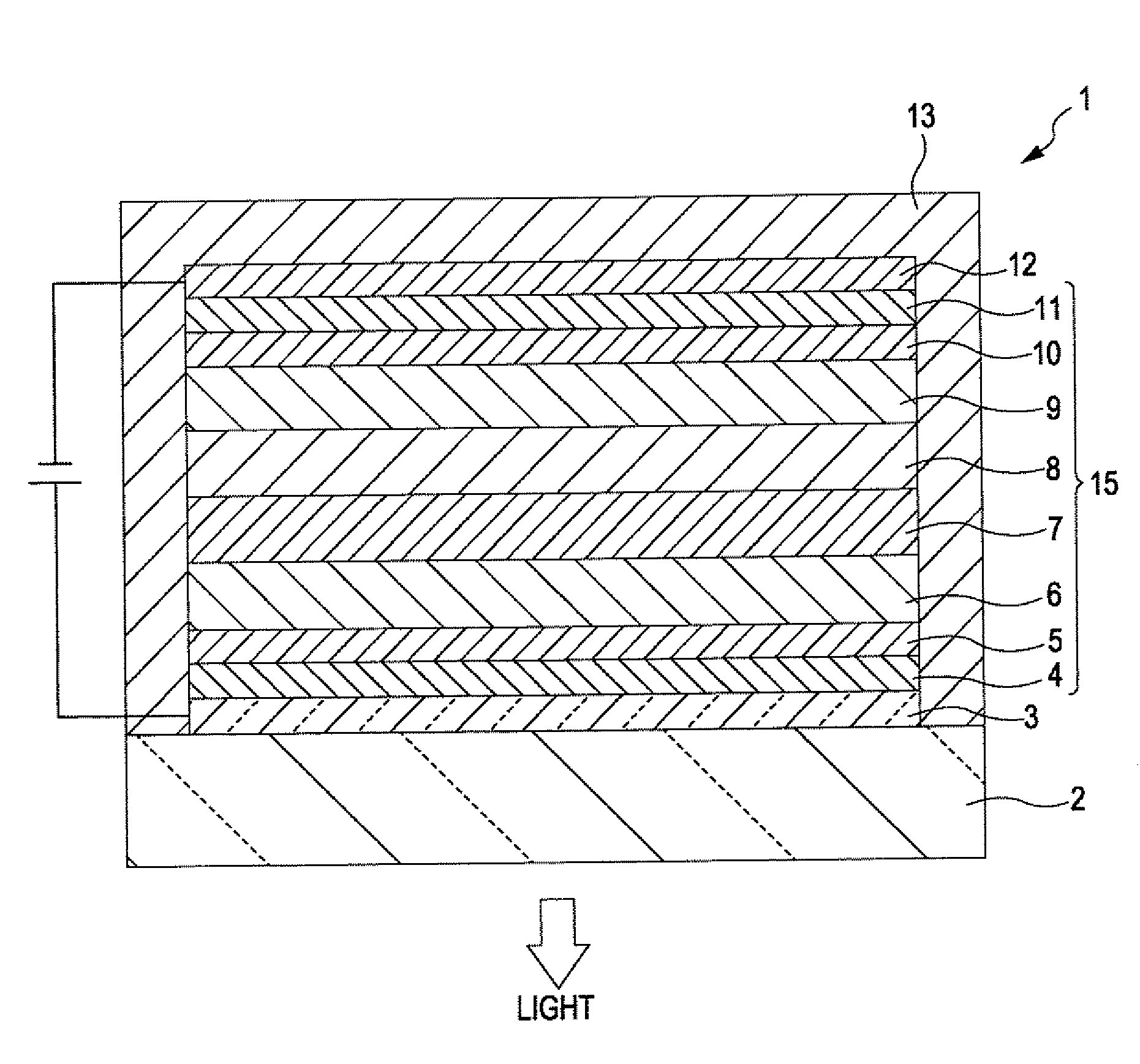
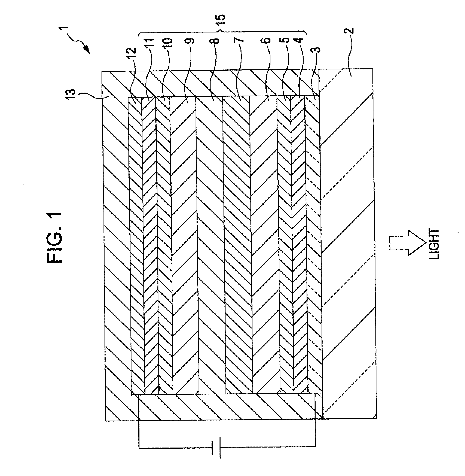
[0044]FIG. 1 is a longitudinal sectional view schematically showing a light-emitting device according to a first embodiment of the invention. For convenience of illustration, the top of FIG. 1 is referred to as the “top” of the device, whereas the bottom of FIG. 1 is referred to as the “bottom” of the device.

[0045]Referring to FIG. 1, a light-emitting device (EL device) 1 emits white light by combining red (R) light, green (G) light, and blue (B) light.

[0046]The light-emitting device 1 includes an anode 3, a hole-injecting layer 4, a hole-transporting layer 5, a red light-emitting layer (first light-emitting layer) 6, an intermediate layer 7, a blue light-emitting layer (second light-emitting layer) 8, a green light-emitting layer (third light-emitting layer) 9, an electron-transporting layer 10, an electron-injecting layer 11, and a cathode 12 that are stacked in the above order.

[0047]In other words, the light-emitting device 1 includes a laminate 15 formed between the two electrod...

second embodiment

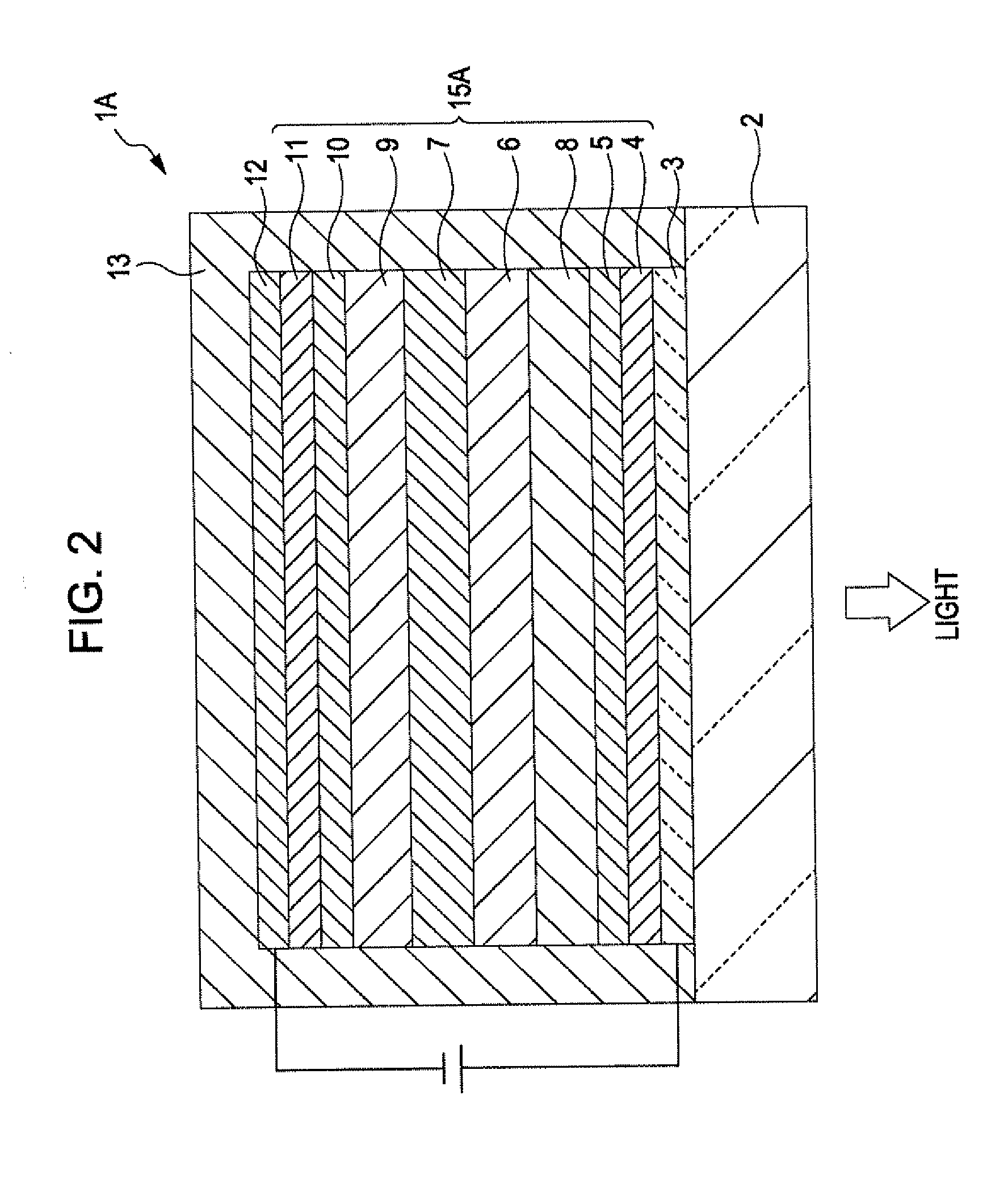
[0167]FIG. 2 is a longitudinal sectional view schematically showing a light-emitting device according to a second embodiment of the invention. For convenience of illustration, the top of FIG. 2 is referred to as the “top” of the device, whereas the bottom of FIG. 2 is referred to as the “bottom” of the device.

[0168]A light-emitting device 1A according to this embodiment is the same as the light-emitting device 1 according to the first embodiment except that the light-emitting layers 6, 8, and 9 and the intermediate layer 7 are stacked in a different order.

[0169]Referring to FIG. 2, the anode 3, the hole-injecting layer 4, the hole-transporting layer 5, the blue light-emitting layer (third light-emitting layer) 8, the red light-emitting layer (first light-emitting layer) 6, the intermediate layer 7, the green light-emitting layer (second light-emitting layer) 9, the electron-transporting layer 10, the electron-injecting layer 11, and the cathode 12 are stacked on the substrate 2 in t...

example 1

[0210](1) First, a transparent glass substrate with an average thickness of 0.5 mm was prepared. An ITO electrode (anode) with an average thickness of 100 nm was formed on the substrate by sputtering.

[0211]The substrate was dipped in acetone and then in 2-propanol and was subjected to ultrasonic cleaning before the substrate was subjected to oxygen plasma treatment.

[0212](2) Next, a hole-injecting layer with an average thickness of 40 nm was formed on the ITO electrode by vacuum deposition using HI406 (manufactured by Idemitsu Kosan Co., Ltd.).

[0213](3) Next, a hole-transporting layer with an average thickness of 20 nm was formed on the hole-injecting layer by vacuum deposition using HT320 (manufactured by Idemitsu Kosan Co., Ltd.).

[0214](4) Next, a red light-emitting layer (first light-emitting layer) with an average thickness of 10 nm was formed on the hole-transporting layer by vacuum deposition using the material of the red light-emitting layer. The material of the red light-emi...


PUM


Abstract

A light-emitting device includes a cathode, an anode, a first light-emitting layer that is disposed between the cathode and the anode and that emits light of a first color, a second light-emitting layer that is disposed between the first light-emitting layer and the cathode and that emits light of a second color different from the first color, and an intermediate layer that is disposed between and in contact with the first light-emitting layer and the second light-emitting layer and that functions to prevent energy transfer of excitons between the first light-emitting layer and the second light-emitting layer. The intermediate layer contains an acene-based material and an amine-based material.

Description

BACKGROUND[0001]1. Technical Field[0002]The present invention relates to light-emitting devices, displays, and electronic apparatuses.[0003]2. Related Art[0004]An organic electroluminescent (EL) device is a light-emitting device including at least one organic light-emitting layer between an anode and a cathode. In this type of light-emitting device, an electric field is applied between the anode and the cathode to inject electrons from the cathode into the light-emitting layer and holes from the anode into the light-emitting layer. The electrons and the holes then recombine together in the light-emitting layer to generate excitons. When the excitons return to the ground state, their energy is released in the form of light.[0005]One such light-emitting device includes three light-emitting layers, corresponding to red (R), green (G), and blue (B), that are stacked between the anode and the cathode so that the device can emit white light (for example, see JP-A-2006-172762 (Patent Docum...

Claims


Application Information

Patent Timeline
Patent Type & Authority Applications(United States)
IPC IPC(8): H01J1/63
CPCH01L27/322H01L27/3244H01L2251/5315H01L51/5036H01L2251/308H01L51/50H10K59/38H10K59/12H10K50/125H10K2102/3026H10K2102/103H10K50/10H05B33/22H10K50/00
Inventor MITSUYA, MASAYUKIYASUKAWA, KOJI
Owner SEIKO EPSON CORP
Learn More