Chalcopyrite type solar cell

a solar cell and chalcopyrite technology, applied in the field of chalcopyrite solar cells, can solve the problems of difficult selenization to a composition, high energy efficiency, and inability to set the temperature during selenization of the precursor, and achieve the effects of avoiding linear scratching, high flexibility, and easy formation

Active Publication Date: 2009-03-12
HONDA MOTOR CO LTD
View PDF8 Cites 52 Cited by
  • Summary
  • Abstract
  • Description
  • Claims
  • Application Information

AI Technical Summary

Benefits of technology

[0030]According to the invention, through holes which penetrate in the stacking direction are disposed as the second scribe portions. According to the configuration, it is not required to form the through holes so as be linearly continuous. Even when a metal stylus or the like is used in disposition of the second scribe portions to perform a mechanical scribing process, therefore, it is possible to avoid formation of a linear scratch in the mica substrate. Accordingly, it is possible to configure a chalcopyrite solar cell in which the bending rigidity is of the mica substrate ensured, and which is highly flexible in accordance with the flexibility of the mica substrate.
[0031]Furthermore, through holes can be formed easily as compared with the case where a linear cutout portion is disposed, and the work ends in a short time. Therefore, the production efficiency of the chalcopyrite solar cell can be improved.

Problems solved by technology

When the glass substrate 12 is used, however, the temperature during the selenization of the precursor cannot be set high.
Therefore, it is difficult to advance the selenization to a composition at which the energy efficiency is very high.
Since the substrate is thick, there are disadvantages that a feeding apparatus for feeding the glass substrate 12 during production of the chalcopyrite solar cell 10, and the like become large, and that the mass of the produced chalcopyrite solar cell 10 is large.
Moreover, the glass substrate 12 is not substantially flexible, and hence it is difficult to apply a mass production method which is called a roll-to-roll process.

Method used


Image

  • Chalcopyrite type solar cell
  • Chalcopyrite type solar cell
  • Chalcopyrite type solar cell

Examples


Embodiment Construction

[0060]Hereinafter, a preferred embodiment of the chalcopyrite solar cell of the invention will be described in detail with reference to the accompanying drawings. Components which are identical with those shown in FIGS. 7 to 10 are denoted by the same reference numerals, and their detailed description is omitted.

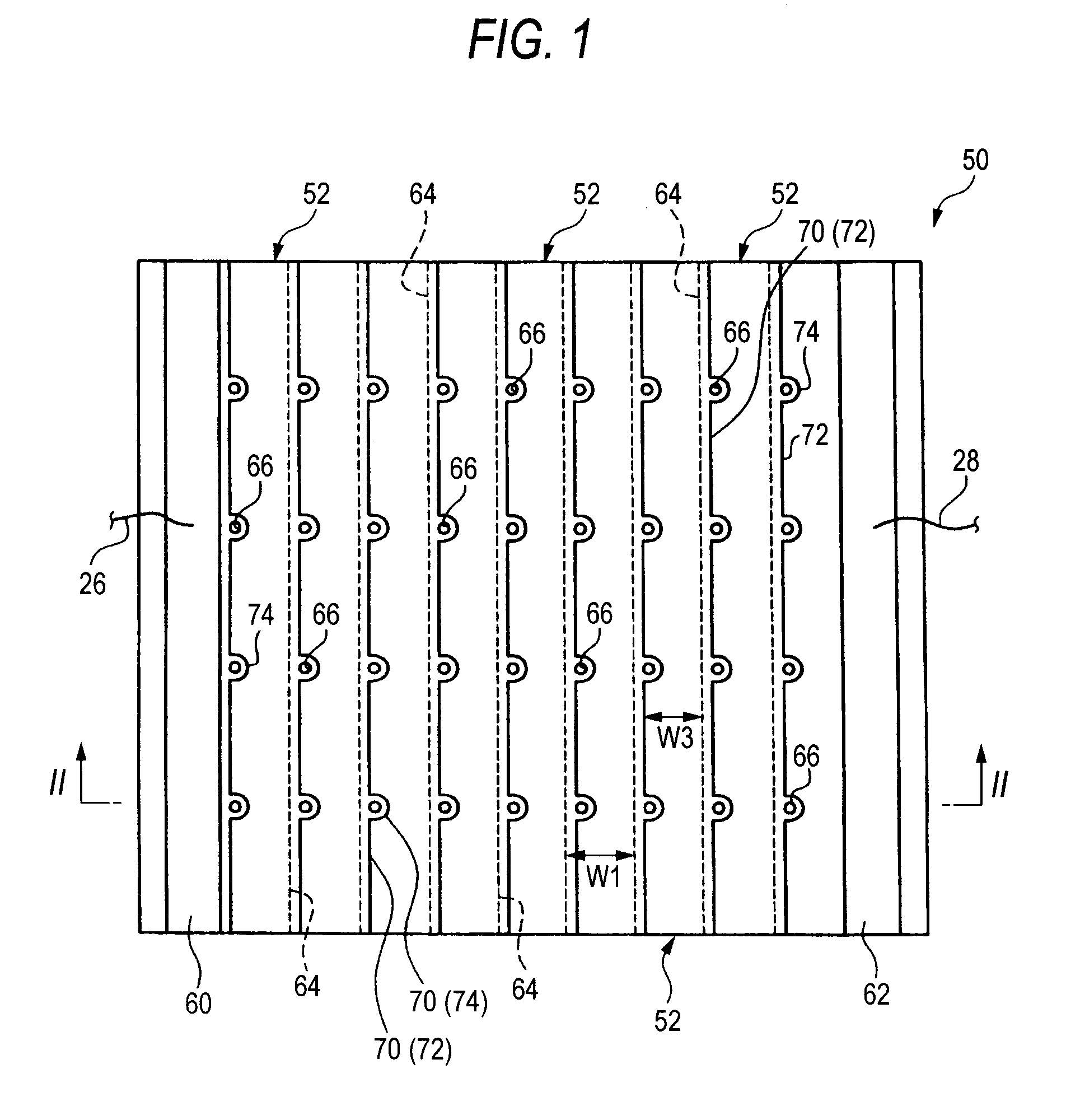
[0061]FIG. 1 is an upper plan view of a chalcopyrite solar cell 50 of the embodiment, and FIG. 2 is a sectional view taken along the line II-II of FIG. 1. The chalcopyrite solar cell 50 is configured by electrically connecting plural unit cells 52 in series to one other.

[0062]Referring to FIG. 2, first, the stacked structure of the unit cells 52 will be described. Each of the unit cells 52 is configured by stacking a binder layer 56 of a nitride, the first electrode layer 14, the P-type light absorbing layer 16 made of a chalcopyrite compound, the buffer layer 18, and a second electrode layer 20 which is transparent and of the n type, on a mica substrate 54 in this sequence....


PUM


Abstract

A first electrode layer 14 is formed on a mica substrate 54, and then first scribe portions 64 are disposed. Next, a light absorbing layer 16 and a buffer layer 18 are disposed on the first electrode layer 14, and through holes (second scribe portions 66) which penetrate from the upper end face of the buffer layer 18 to the lower end face of the mica substrate 54 are formed in a spot-like manner. Then, a second electrode layer 20 is disposed on the buffer layer 18. At this time, the lower end face of the second electrode layer 20 reaches the first electrode layer 14 along the inner peripheral walls of the second scribe portions 66. Furthermore, the second electrode layer 20 is scribed to dispose third scribe portions 70.

Description

TECHNICAL FIELD[0001]The present invention relates to a chalcopyrite solar cell, and more particularly to a chalcopyrite solar cell in which adjacent unit cells are electrically connected in series to one other to configure one module.BACKGROUND ART[0002]FIG. 7 is a side view in the stacking direction of a usual chalcopyrite solar cell 10. The chalcopyrite solar cell 10 is configured by disposing a first electrode layer 14 made of Mo, a light absorbing layer 16 made of Cu(InGa)Se (hereinafter, often referred to as CIGS), a buffer layer 18 made of CdS, ZnO, InS, or the like, and a transparent second electrode layer 20 made of ZnO / Al on a glass substrate 12 in this sequence. In FIG. 7, the reference numerals 22, 24 denote a first lead portion and a second lead portion, and lead wires 26, 28 are connected to the lead portions 22, 24.[0003]In this way, the chalcopyrite solar cell 10 is a solar cell comprising a chalcopyrite compound which is typified by CIGS, as the light absorbing laye...

Claims


Application Information

Patent Timeline
IPC IPC(8): H01L31/042B05D5/12
CPCH01L31/0392H01L31/03928H01L31/046H01L31/0749Y02E10/541H01L31/042H01L31/0465Y02P70/50
Inventor YONEZAWA, SATOSHIHAYASHIDA, TADASHI
Owner HONDA MOTOR CO LTD
Why Eureka
Try Eureka