
Multilayer ceramic circuit board having protruding portion and method for manufacturing the same

a ceramic circuit board and ceramic technology, applied in printed circuits, printed circuit aspects, printed circuit stress/warp reduction, etc., can solve problems such as disposal, and achieve the effect of increasing flatness

Inactive Publication Date: 2009-03-05
ALPS ALPINE CO LTD
View PDF13 Cites 8 Cited by
  • Summary
  • Abstract
  • Description
  • Claims
  • Application Information

AI Technical Summary

Benefits of technology

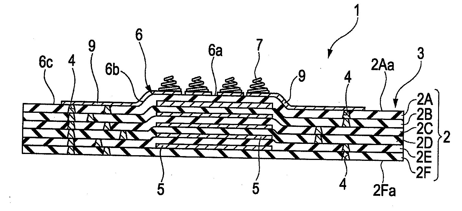
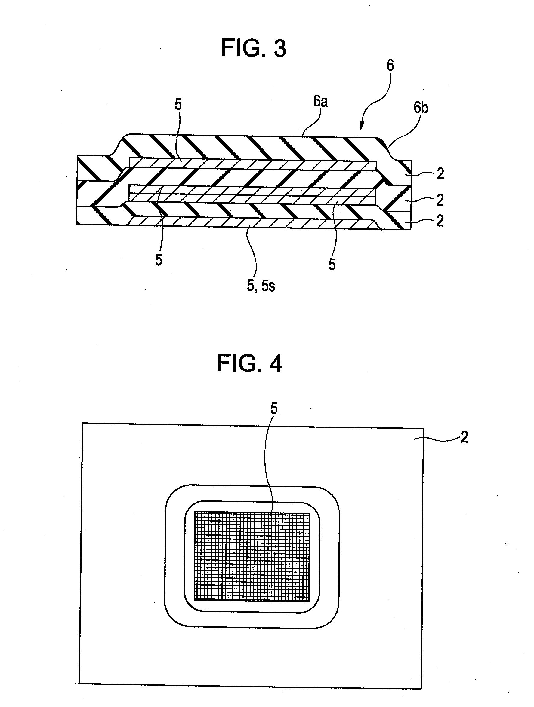
[0011]In the multilayer ceramic circuit board according to the first aspect, the one or two or more lifting layers lying below swell the top ceramic wiring layer such that the protruding portion protrudes, and therefore the side of the protruding portion can be smoothly inclined. Furthermore, since the one or two or more lifting layers used for protruding the protruding portion have a planar shape, the protruding portion-formed surface can have high flatness, regardless of the size of protruding portion-formed surface corresponding to the top surface of the protruding portion.
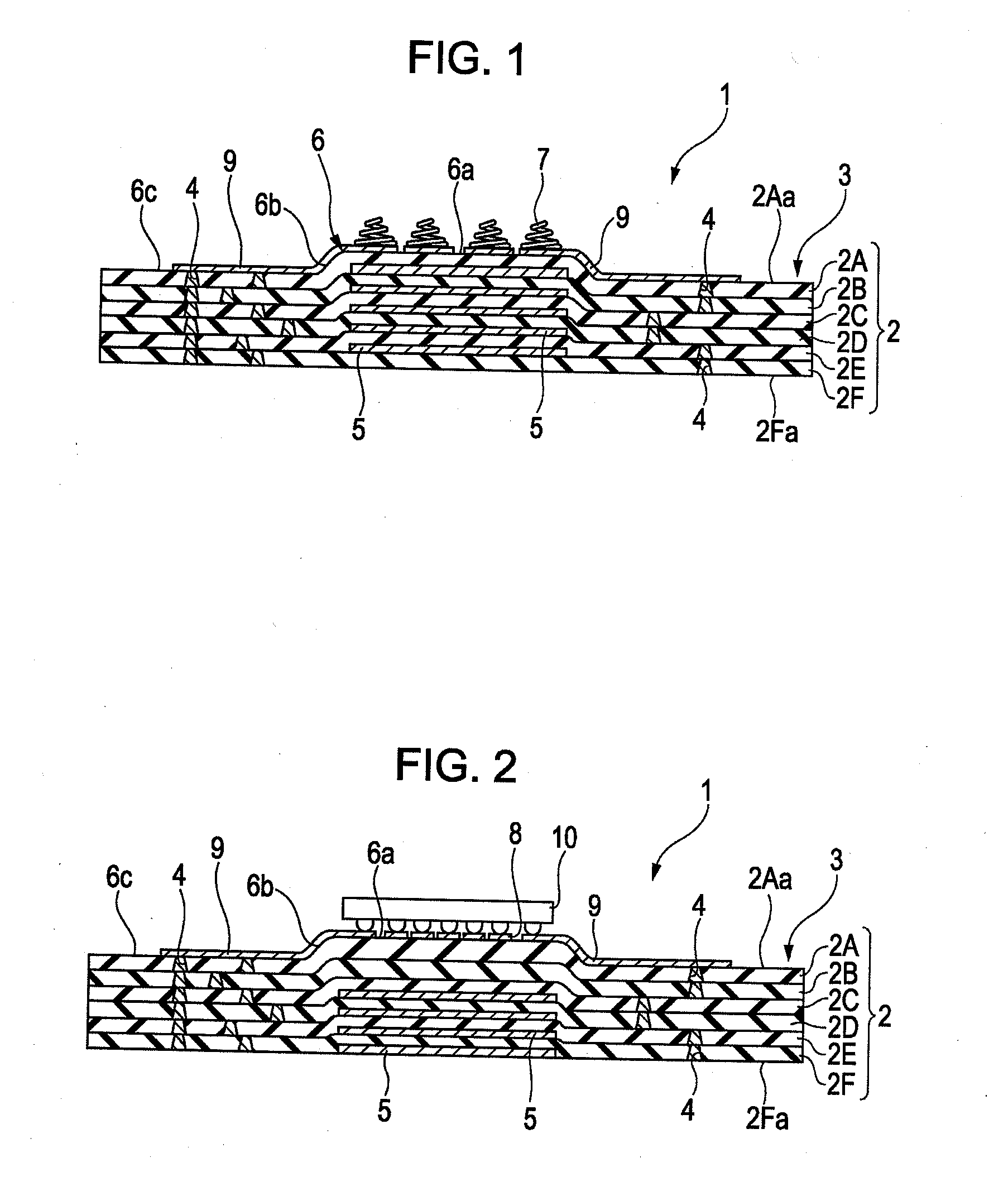
[0014]According to the first and second aspects of the present invention, in the multilayer ceramic circuit board and the method for manufacturing the multilayer ceramic circuit board, since a protruding portion is formed using a planar lifting layer or layers and increasing the number of stacked layers partially in the multilayer ceramic circuit board, it is possible to provide a multilayer ceramic circuit board in which the protruding portion smoothly protrudes and the flatness is increased.

Problems solved by technology

In the first method for forming the protruding portion 106, however, as shown in FIG. 8, since the side of the protruding portion 106 is steep, it is not possible to dispose a wiring pattern continuously so as to extend from the region provided with the protruding portion 106 to the region not provided with the protruding portion 106 via the side of the protruding portion 106, which is a problem.

Method used


Image

  • Multilayer ceramic circuit board having protruding portion and method for manufacturing the same
  • Multilayer ceramic circuit board having protruding portion and method for manufacturing the same
  • Multilayer ceramic circuit board having protruding portion and method for manufacturing the same

Examples


Embodiment Construction

[0027]A multilayer ceramic circuit board and a method for manufacturing the multilayer ceramic circuit board according to an embodiment of the present invention will be described below with reference to the drawings.

[0028]FIGS. 1 and 2 are each a longitudinal sectional view showing a multilayer ceramic circuit board 1 according to the embodiment. As shown in FIG. 1, the multilayer ceramic circuit board 1 includes a plurality of ceramic wiring layers 2 and lifting layers 5.

[0029]The plurality of ceramic wiring layers 2 are stacked vertically as shown in FIG. 1. In the multilayer ceramic circuit board 1 according to this embodiment, six ceramic wiring layers 2 are stacked. A top ceramic wiring layer 2A is designated as a first ceramic wiring layer 2A, and a bottom ceramic wiring layer 2F is designated as a sixth ceramic wiring layer 2F. The ceramic wiring layers are designated from the top to the bottom by a first ceramic wiring layer 2A, a second ceramic wiring layer 2B, . . . , a si...


PUM

PropertyMeasurementUnit
thicknessaaaaaaaaaa
widthaaaaaaaaaa
lengthaaaaaaaaaa

Abstract

A multilayer ceramic circuit board includes ceramic wiring layers which are stacked together, one or two or more lifting layers which have a planar shape and which are disposed as an inner layer inside the stacked ceramic wiring layers or as a lower layer lower than a bottom ceramic wiring layer, and a protruding portion formed on a surface of a top ceramic wiring layer due to the disposition of the one or two or more lifting layers. The protruding portion smoothly protrudes and has a large area and high flatness. The multilayer ceramic circuit board is formed by disposing lifting layers as an inner layer of a plurality green sheets or as a lower layer lower than a bottom green sheet, and firing under pressure the resulting laminate in a state constrained by an elastic constraining sheet and a rigid constraining sheet.

Description

CLAIM OF PRIORITY[0001]This application claims benefit of the Japanese Patent Application No. 2007-230447 filed on Sep. 5, 2007, which is hereby incorporated by reference in its entirety.BACKGROUND OF THE INVENTION[0002]1. Field of the Invention[0003]The present invention relates to a multilayer ceramic circuit board and a method for manufacturing the multilayer ceramic circuit board. More particularly, the invention relates to a multilayer ceramic circuit board which is suitable for use when protruding portions are provided on the surface of the multilayer ceramic circuit board, and a method for manufacturing the multilayer ceramic circuit board.[0004]2. Description of the Related Art[0005]FIG. 8 shows an example of a multilayer ceramic circuit board 101 according to the related art. The multilayer ceramic circuit board 101 is formed by stacking a plurality of ceramic wiring layers 102. A protruding portion 106 is disposed on the surface of the multilayer ceramic circuit board 101 ...

Claims


Application Information

Patent Timeline
Patent Type & Authority Applications(United States)
IPC IPC(8): H05K1/00B32B37/06
CPCH01L21/4807H05K2201/2009H01L23/49811H01L23/49822H01L23/49827H01L2224/16225H01L2924/0102H01L2924/01078H01L2924/01079H01L2924/09701H01L2924/3025H05K1/0271H05K1/0306H05K1/111H05K3/0014H05K3/4007H05K3/4611H05K3/4629H05K2201/0195H05K2201/0367H05K2201/09045H05K2201/09781H01L23/15
Inventor MIURA, HISAOMURATA, SHINJI
Owner ALPS ALPINE CO LTD
Learn More